SNVS603D August 2009 – July 2019 LM3424
PRODUCTION DATA.
- 1 Features
- 2 Applications
- 3 Description
- 4 Revision History
- 5 Pin Configuration and Functions
- 6 Specifications
-
7 Detailed Description
- 7.1 Overview
- 7.2 Functional Block Diagram
- 7.3
Feature Description
- 7.3.1 Current Regulators
- 7.3.2 Peak Current Mode Control
- 7.3.3 Average LED Current
- 7.3.4 Thermal Foldback and Analog Dimming
- 7.3.5 Current Sense and Current Limit
- 7.3.6 Slope Compensation
- 7.3.7 Control Loop Compensation
- 7.3.8 Start-Up Regulator and Soft-Start
- 7.3.9 Overvoltage Lockout (OVLO)
- 7.3.10 Input Undervoltage Lockout (UVLO)
- 7.3.11 PWM Dimming
- 7.3.12 Thermal Shutdown
- 7.4 Device Functional Modes
-
8 Application and Implementation
- 8.1 Application Information
- 8.2
Typical Applications
- 8.2.1
Basic Topology Schematics
- 8.2.1.1 Design Requirements
- 8.2.1.2
Detailed Design Procedure
- 8.2.1.2.1 Operating Point
- 8.2.1.2.2 Switching Frequency
- 8.2.1.2.3 Average LED Current
- 8.2.1.2.4 Thermal Foldback
- 8.2.1.2.5 Inductor Ripple Current
- 8.2.1.2.6 LED Ripple Current
- 8.2.1.2.7 Peak Current Limit
- 8.2.1.2.8 Slope Compensation
- 8.2.1.2.9 Loop Compensation
- 8.2.1.2.10 Input Capacitance
- 8.2.1.2.11 NFET
- 8.2.1.2.12 Diode
- 8.2.1.2.13 Output OVLO
- 8.2.1.2.14 Input UVLO
- 8.2.1.2.15 Soft-Start
- 8.2.1.2.16 PWM Dimming Method
- 8.2.1.2.17 Analog Dimming Method
- 8.2.2
Buck-Boost Application
- 8.2.2.1 Design Requirements
- 8.2.2.2
Detailed Design Procedure
- 8.2.2.2.1 Operating Point
- 8.2.2.2.2 Switching Frequency
- 8.2.2.2.3 Average LED Current
- 8.2.2.2.4 Thermal Foldback
- 8.2.2.2.5 Inductor Ripple Current
- 8.2.2.2.6 Output Capacitance
- 8.2.2.2.7 Peak Current Limit
- 8.2.2.2.8 Slope Compensation
- 8.2.2.2.9 Loop Compensation
- 8.2.2.2.10 Input Capacitance
- 8.2.2.2.11 NFET
- 8.2.2.2.12 Diode
- 8.2.2.2.13 Input UVLO
- 8.2.2.2.14 Output OVLO
- 8.2.2.2.15 Soft-Start
- 8.2.2.3 Application Curve
- 8.2.3 Boost Application
- 8.2.4 Buck-Boost Application
- 8.2.5 Boost Application
- 8.2.6 Buck-Boost Application
- 8.2.7 Buck Application
- 8.2.8 Buck-Boost Application
- 8.2.9 SEPIC Application
- 8.2.1
Basic Topology Schematics
- 9 Power Supply Recommendations
- 10Layout
- 11Device and Documentation Support
- 12Mechanical, Packaging, and Orderable Information
Package Options
Mechanical Data (Package|Pins)
- PWP|20
Thermal pad, mechanical data (Package|Pins)
- PWP|20
Orderable Information
7.3.6 Slope Compensation
The LM3424 has programmable slope compensation in order to provide stability over a wide range of operating conditions. Without slope compensation, a well-known condition called current mode instability (or sub-harmonic oscillation) can result if there is a perturbation of the MOSFET current sense voltage at the IS pin, due to noise or a some type of transient.
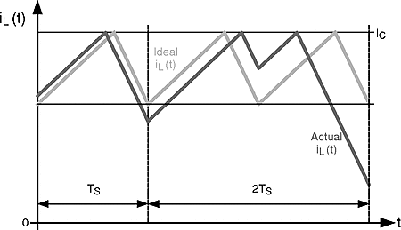
Through a mathematical / geometrical analysis of the inductor current (IL) and the corresponding control current (IC, it can be shown that if D < 0.5, the effect of the perturbation will decrease each switching cycle and the system will remain stable. However, if D > 0.5 then the perturbation will grow as shown in Figure 23, eventually causing a "period doubling" effect where the effect of the perturbation remains, yielding current mode instability.
Looking at Figure 22, the positive PWM comparator input is the IS voltage, a mirror of IL during tON, plus a typical 900 mV offset. The negative input of the PWM comparator is the COMP pin which is proportional to IC, the threshold at which the main MOSFET (Q1) is turned off.
The LM3424 mitigates current mode instability by implementing an aritifical ramp (commonly called slope compensation) which is summed with the sensed MOSFET current at the IS pin as shown in Figure 22. This combined signal is compared to the COMP pin to generate the PWM signal. An increase in the ramp that is added to the sense voltage will increase the maximum achievable duty cycle. It should be noted that as the artificial ramp is increased more and more, the control method approaches standard voltage mode control and the benefits of current mode control are reduced.
To program the slope compensation, an external resistor, RSLP, is connected from SLOPE to GND. This sets the slope of the artificial ramp that is added to the MOSFET current sense voltage. A smaller RSLP value will increase the slope of the added ramp. A simple calculation is suggested to ensure any duty cycle is attainable while preventing the addition of excessive ramp. This method requires the artifical ramp slope (MA) to be equal to half the inductor slope during tOFF:

 Figure 23. "Period Doubling" due to Current Mode Instability