SNVSB12B November 2017 – May 2021 LM73605-Q1 , LM73606-Q1
PRODUCTION DATA
- 1 Features
- 2 Applications
- 3 Description
- 4 Revision History
- 5 Device Comparison
- 6 Pin Configuration and Functions
- 7 Specifications
-
8 Detailed Description
- 8.1 Overview
- 8.2 Functional Block Diagram
- 8.3
Feature Description
- 8.3.1 Synchronous Step-Down Regulator
- 8.3.2 Auto Mode and FPWM Mode
- 8.3.3 Fixed-Frequency Peak Current-Mode Control
- 8.3.4 Adjustable Output Voltage
- 8.3.5 Enable and UVLO
- 8.3.6 Internal LDO, VCC_UVLO, and BIAS Input
- 8.3.7 Soft Start and Voltage Tracking
- 8.3.8 Adjustable Switching Frequency
- 8.3.9 Frequency Synchronization and Mode Setting
- 8.3.10 Internal Compensation and CFF
- 8.3.11 Bootstrap Capacitor and VBOOT-UVLO
- 8.3.12 Power-Good and Overvoltage Protection
- 8.3.13 Overcurrent and Short-Circuit Protection
- 8.3.14 Thermal Shutdown
- 8.4 Device Functional Modes
- 9 Layout
- 10Device and Documentation Support
Package Options
Mechanical Data (Package|Pins)
- RNP|30
Thermal pad, mechanical data (Package|Pins)
- RNP|30
Orderable Information
8.3.8 Adjustable Switching Frequency
The internal oscillator frequency is controlled by the impedance on the RT pin. If the RT pin is open circuit, the LM73605-Q1/6-Q1 at default switching frequency, 500 kHz. The RT pin is not designed to be connected directly to ground. To program the switching frequency by RT resistor, Equation 13, or Figure 8-12, or Table 8-1 can be used to find the resistance value.
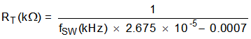
 Figure 8-12 RT Resistance versus Switching Frequency
| SWITCHING FREQUENCY fSW (kHz) | RT RESISTANCE (kΩ) |
| 350 | 115 |
| 400 | 100 |
| 500 | 78.7 (or open) |
| 750 | 52.3 |
| 1000 | 39.2 |
| 1500 | 26.1 |
| 2000 | 19.1 |
| 2200 | 17.4 |
The choice of switching frequency is usually a compromise between conversion efficiency and the size of the solution. Lower switching frequency has lower switching losses (including gate charge losses, switch transition losses, and so forth) and usually results in higher overall efficiency. However, higher switching frequency allows the use of smaller power inductor and output capacitors, hence a more compact design. Lower inductance also helps transient response (higher large signal slew rate of inductor current), and has lower DCR. The optimal switching frequency is usually a trade-off in a given application and thus needs to be determined on a case-by-case basis. The following are factors that need to be taken into account:
- Input voltage range
- Output voltage
- Most frequent load current level or levels
- External component choices
- Solution size/cost requirements
- Efficiency
- Thermal management requirements
The choice of switching frequency can also be limited whether an operating condition triggers tON-MIN or tOFF-MIN. Minimum on-time, tON-MIN, is the smallest time that the HS switch can be on. Minimum off-time, tOFF-MIN, is the smallest duration that the HS switch can be off.
In CCM operation, tON-MIN and tOFF_MIN limit the voltage conversion range given a selected switching frequency, fSW. The minimum duty cycle allowed is:
The maximum duty cycle allowed is:
Given an output voltage, the choice of the switching frequency affects the allowed input voltage range, solution size and efficiency. The maximum operational supply voltage can be found by:
At lower supply voltage, the switching frequency decreases once tOFF-MIN is tripped. The minimum VIN without frequency foldback can be approximated by:
With a desired VOUT, the range of allowed VIN is narrower with higher switching frequency.
The LM73605-Q1/6-Q1 an advanced frequency foldback algorithm under both tON_MIN and tOFF_MIN conditions. With frequency foldback, stable output voltage regulation is extended to wider range of supply voltages.
At very high VIN conditions where tON-MIN limitation is met, the switching frequency reduces to allow higher VIN while maintaining VOUT regulation. Note that the peak-to-peak inductor current ripple will increase with higher VIN and lower frequency. TI does not recommend designing the circuit to operate with tON_MIN under typical conditions.
At very low VIN conditions, where tOFF-MIN limitation is met, the switching frequency decreases until tON-MAX condition is met. Such frequency foldback mechanism allows the LM73605-Q1/6-Q1 to have very low dropout voltage regardless of frequency setting.