SNVSB12B November 2017 – May 2021 LM73605-Q1 , LM73606-Q1
PRODUCTION DATA
- 1 Features
- 2 Applications
- 3 Description
- 4 Revision History
- 5 Device Comparison
- 6 Pin Configuration and Functions
- 7 Specifications
-
8 Detailed Description
- 8.1 Overview
- 8.2 Functional Block Diagram
- 8.3
Feature Description
- 8.3.1 Synchronous Step-Down Regulator
- 8.3.2 Auto Mode and FPWM Mode
- 8.3.3 Fixed-Frequency Peak Current-Mode Control
- 8.3.4 Adjustable Output Voltage
- 8.3.5 Enable and UVLO
- 8.3.6 Internal LDO, VCC_UVLO, and BIAS Input
- 8.3.7 Soft Start and Voltage Tracking
- 8.3.8 Adjustable Switching Frequency
- 8.3.9 Frequency Synchronization and Mode Setting
- 8.3.10 Internal Compensation and CFF
- 8.3.11 Bootstrap Capacitor and VBOOT-UVLO
- 8.3.12 Power-Good and Overvoltage Protection
- 8.3.13 Overcurrent and Short-Circuit Protection
- 8.3.14 Thermal Shutdown
- 8.4 Device Functional Modes
- 9 Layout
- 10Device and Documentation Support
Package Options
Mechanical Data (Package|Pins)
- RNP|30
Thermal pad, mechanical data (Package|Pins)
- RNP|30
Orderable Information
8.3.4 Adjustable Output Voltage
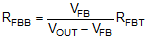
The voltage regulation loop in the LM73605-Q1/6-Q1 the FB pin voltage to be the same as the internal reference voltage. The output voltage of the LM73605-Q1/6-Q1 is set by a resistor divider to program the ratio from VOUT to VFB. The resistor divider is connected from the output to ground with the mid-point connecting to the FB pin.
 Figure 8-4 Output Voltage Setting by Resistor Divider
The internal voltage reference and feedback loop produce precise voltage regulation over temperature. TI recommends using divider resistors with 1% tolerance or better, and with temperature coefficient of 100 ppm or lower. Typically, RFBT = 10 kΩ to 100 kΩ is recommended. Larger RFBT and RFBB values reduce the quiescent current going through the divider, which help maintain high efficiency at very light load. Larger divider values also make the feedback path more susceptible to noise. If efficiency at very light load is critical in a certain application, RFBT up to 1 MΩ can be used.
RFBB can be calculated by Equation 7:
The minimum programmable VOUT equals VFB, with RFBB open. The maximum VOUT is limited by the maximum duty cycle at a given frequency:
where
- tOFF-MIN is the minimum off time of the HS switch
- TSW = 1 / fSW is the switching period
Ideally, without frequency foldback, VOUT_MAX = VIN_MIN × DMAX.
Power losses in the circuit reduces the maximum output voltage. The LM73605-Q1/6-Q1 back switching frequency under tOFF_MIN condition to further extend VOUT_MAX. The device maintains output regulation with lower input voltage. The minimum foldback frequency is limited by the maximum HS on-time, tON_MAX. Maximum output voltage with frequency foldback can be estimated by:

The voltage drops on the HS MOSFET and inductor DCR have been taken into account in Equation 9. The switching losses were not included.
If the resistor divider is not connected properly, the output voltage cannot be regulated because the feedback loop cannot obtain correct output voltage information. If the FB pin is shorted to ground or disconnected, the output voltage is driven close to VIN. The load connected to the output can be damaged under this condition. Do not short FB to ground or leave it open circuit during operation.
The FB pin is a noise sensitive node. It is important to place the resistor divider as close as possible to the FB pin, and route the feedback node with a short and thin trace. The trace connecting VOUT to RFBT can be long, but it must be routed away from the noisy area of the PCB. For more layout recommendations, see the Section 9 section.