SNVSB12B November 2017 – May 2021 LM73605-Q1 , LM73606-Q1
PRODUCTION DATA
- 1 Features
- 2 Applications
- 3 Description
- 4 Revision History
- 5 Device Comparison
- 6 Pin Configuration and Functions
- 7 Specifications
-
8 Detailed Description
- 8.1 Overview
- 8.2 Functional Block Diagram
- 8.3
Feature Description
- 8.3.1 Synchronous Step-Down Regulator
- 8.3.2 Auto Mode and FPWM Mode
- 8.3.3 Fixed-Frequency Peak Current-Mode Control
- 8.3.4 Adjustable Output Voltage
- 8.3.5 Enable and UVLO
- 8.3.6 Internal LDO, VCC_UVLO, and BIAS Input
- 8.3.7 Soft Start and Voltage Tracking
- 8.3.8 Adjustable Switching Frequency
- 8.3.9 Frequency Synchronization and Mode Setting
- 8.3.10 Internal Compensation and CFF
- 8.3.11 Bootstrap Capacitor and VBOOT-UVLO
- 8.3.12 Power-Good and Overvoltage Protection
- 8.3.13 Overcurrent and Short-Circuit Protection
- 8.3.14 Thermal Shutdown
- 8.4 Device Functional Modes
- 9 Layout
- 10Device and Documentation Support
Package Options
Mechanical Data (Package|Pins)
- RNP|30
Thermal pad, mechanical data (Package|Pins)
- RNP|30
Orderable Information
8.3.12 Power-Good and Overvoltage Protection
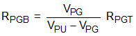
The LM73605-Q1/6-Q1 a built-in power-good (PGOOD) flag to indicate whether the output voltage is at an appropriate level or not. The PGOOD flag can be used for start-up sequencing of multiple rails. The PGOOD pin is an open-drain output that requires a pullup resistor to an appropriate logic voltage (any voltage below 15 V). The pin can sink 5 mA of current and maintain its specified logic low level. A typical pullup resistor value is 10 kΩ to 100 kΩ. When the FB voltage is higher than VPGOOD-OV or lower than VPGOOD-UV threshold, the PGOOD internal switch is turned on, and the PGOOD pin voltage is pulled low. When the FB is within the range, the PGOOD switch is turned off, and the pin is pulled up to the voltage connected to the pullup resistor. The PGOOD function also has a deglitch timer for about 140 µs for each transition. If it is desired to pull up PGOOD pin to a voltage higher than 15 V, a resistor divider can be used to divide the voltage down.
 Figure 8-15 Divider for PGOOD Pullup Voltage
With a given pullup voltage VPU, select a desired voltage on the PGOOD pin, VPG. With a selected RPGT, the RPGB can be found by:
When the device is disabled, the output voltage is low, and the PGOOD flag indicates logic low as long as VIN > 2 V.