SNVS817B June 2012 – June 2019 LMR12015 , LMR12020
PRODUCTION DATA.
- 1 Features
- 2 Applications
- 3 Description
- 4 Revision History
- 5 Pin Configuration and Functions
- 6 Specifications
- 7 Detailed Description
-
8 Application and Implementation
- 8.1 Application Information
- 8.2
Typical Application
- 8.2.1
Detailed Design Procedure
- 8.2.1.1 Custom Design With WEBENCH® Tools
- 8.2.1.2 Inductor Selection
- 8.2.1.3 Input Capacitor
- 8.2.1.4 Output Capacitor
- 8.2.1.5 Catch Diode
- 8.2.1.6 Boost Diode (Optional)
- 8.2.1.7 Boost Capacitor
- 8.2.1.8 Output Voltage
- 8.2.1.9 Feedforward Capacitor (Optional)
- 8.2.1.10
Calculating Efficiency and Junction Temperature
- 8.2.1.10.1 Schottky Diode Conduction Losses
- 8.2.1.10.2 Inductor Conduction Losses
- 8.2.1.10.3 MOSFET Conduction Losses
- 8.2.1.10.4 MOSFET Switching Losses
- 8.2.1.10.5 IC Quiescent Losses
- 8.2.1.10.6 MOSFET Driver Losses
- 8.2.1.10.7 Total Power Losses
- 8.2.1.10.8 Efficiency Calculation Example
- 8.2.1.10.9 Calculating the LMR2015/20 Junction Temperature
- 8.2.2 Application Curves
- 8.2.3 LMR12015/20 Circuit Examples
- 8.2.1
Detailed Design Procedure
- 9 Layout
- 10Device and Documentation Support
- 11Mechanical, Packaging, and Orderable Information
Package Options
Mechanical Data (Package|Pins)
- DSC|10
Thermal pad, mechanical data (Package|Pins)
- DSC|10
Orderable Information
7.4.1 Enable Pin / Shutdown Mode
Connect the EN pin to a voltage source greater than 1.8V to enable operation of the LMR12015/20. Apply a voltage less than 0.4V to put the part into shutdown mode. In shutdown mode the quiescent current drops to typically 70 nA. Switch leakage adds another 40 nA from the input supply. For proper operation, the LMR12015/20 EN pin should never be left floating, and the voltage should never exceed VIN + 0.3 V.
The simplest way to enable the operation of the LMR12015/20 is to connect the EN pin to AVIN which allows self start-up of the LMR12015/20 when the input voltage is applied.
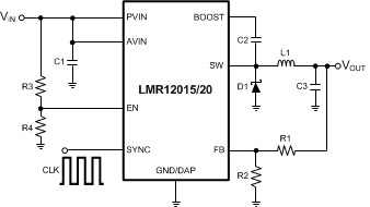
When the rise time of VIN is longer than the soft-start time of the LMR12015/20 this method may result in an overshoot in output voltage. In such applications, the EN pin voltage can be controlled by a separate logic signal, or tied to a resistor divider, which reaches 1.8V after VIN is fully established (see Figure 25). This will minimize the potential for output voltage overshoot during a slow VIN ramp condition. Use the lowest value of VIN , seen in your application when calculating the resistor network, to ensure that the 1.8-V minimum EN threshold is reached.
 Figure 25. Resistor Divider on EN