SNVS817B June 2012 – June 2019 LMR12015 , LMR12020
PRODUCTION DATA.
- 1 Features
- 2 Applications
- 3 Description
- 4 Revision History
- 5 Pin Configuration and Functions
- 6 Specifications
- 7 Detailed Description
-
8 Application and Implementation
- 8.1 Application Information
- 8.2
Typical Application
- 8.2.1
Detailed Design Procedure
- 8.2.1.1 Custom Design With WEBENCH® Tools
- 8.2.1.2 Inductor Selection
- 8.2.1.3 Input Capacitor
- 8.2.1.4 Output Capacitor
- 8.2.1.5 Catch Diode
- 8.2.1.6 Boost Diode (Optional)
- 8.2.1.7 Boost Capacitor
- 8.2.1.8 Output Voltage
- 8.2.1.9 Feedforward Capacitor (Optional)
- 8.2.1.10
Calculating Efficiency and Junction Temperature
- 8.2.1.10.1 Schottky Diode Conduction Losses
- 8.2.1.10.2 Inductor Conduction Losses
- 8.2.1.10.3 MOSFET Conduction Losses
- 8.2.1.10.4 MOSFET Switching Losses
- 8.2.1.10.5 IC Quiescent Losses
- 8.2.1.10.6 MOSFET Driver Losses
- 8.2.1.10.7 Total Power Losses
- 8.2.1.10.8 Efficiency Calculation Example
- 8.2.1.10.9 Calculating the LMR2015/20 Junction Temperature
- 8.2.2 Application Curves
- 8.2.3 LMR12015/20 Circuit Examples
- 8.2.1
Detailed Design Procedure
- 9 Layout
- 10Device and Documentation Support
- 11Mechanical, Packaging, and Orderable Information
Package Options
Mechanical Data (Package|Pins)
- DSC|10
Thermal pad, mechanical data (Package|Pins)
- DSC|10
Orderable Information
8.2.1.9 Feedforward Capacitor (Optional)
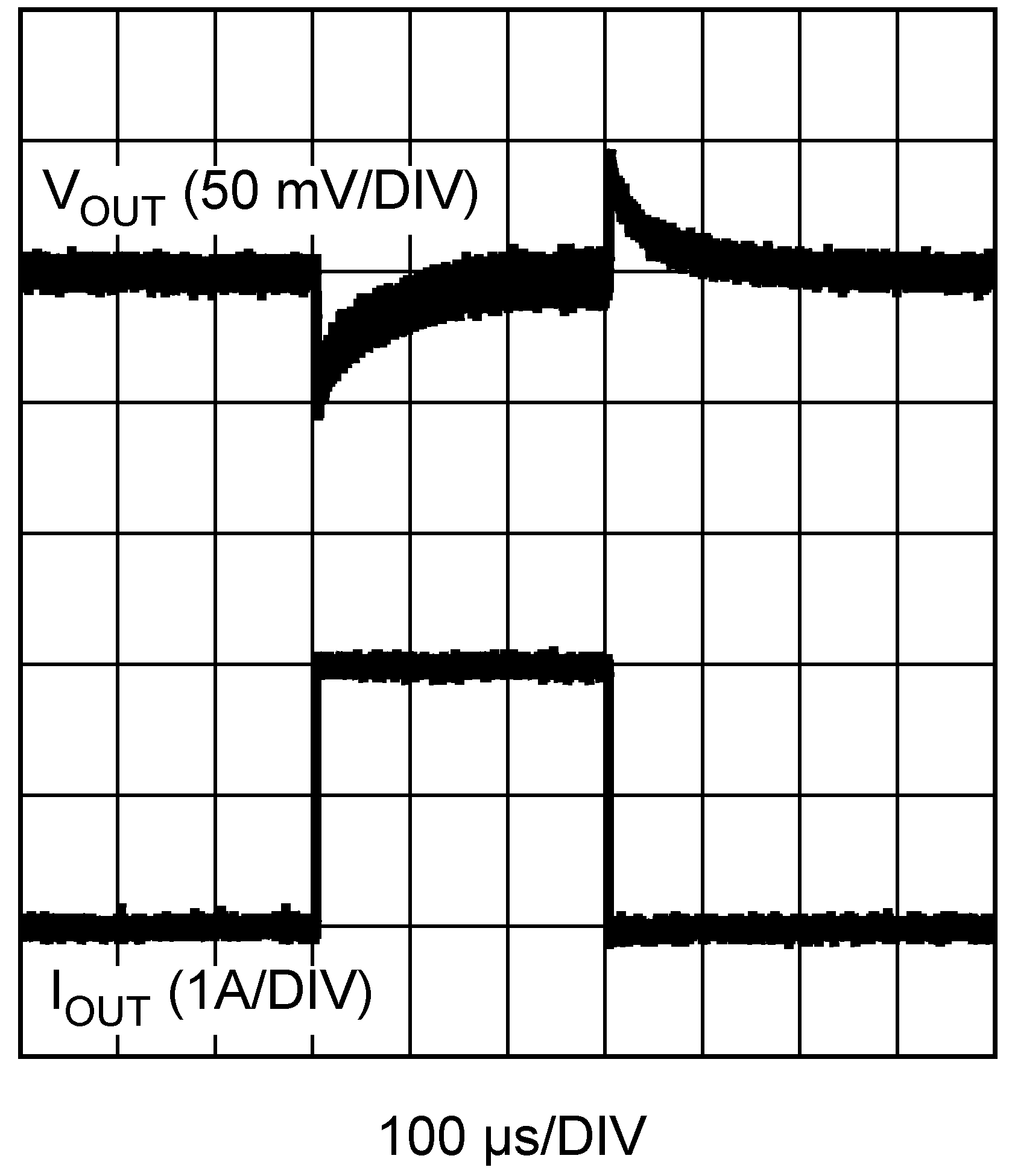
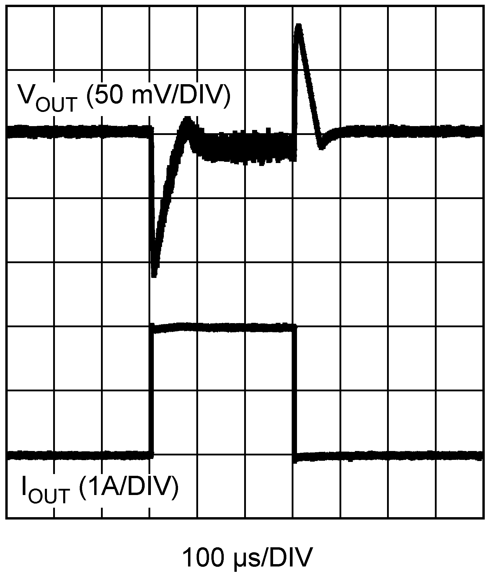
A feed forward capacitor CFF can improve the transient response of the converter. Place CFF in parallel with R1. The value of CFF should place a zero in the loop response at, or above, the pole of the output capacitor and RLOAD. The CFF capacitor will increase the crossover frequency of the design, thus a larger minimum output capacitance is required for designs using CFF. CFF must only be used with an output capacitance greater than or equal to 44 uF. Example waveforms of load transient with and without the CFF capacitorss are as shown below.
Equation 28. 

 Figure 28. LMR12015/20 Load Transient With CFF Capacitor
VOUT = 3.3 V
 Figure 29. LMR12015/20 Load Transient Without CFF Capacitor
VOUT = 3.3 V