SNVS817B June 2012 – June 2019 LMR12015 , LMR12020
PRODUCTION DATA.
- 1 Features
- 2 Applications
- 3 Description
- 4 Revision History
- 5 Pin Configuration and Functions
- 6 Specifications
- 7 Detailed Description
-
8 Application and Implementation
- 8.1 Application Information
- 8.2
Typical Application
- 8.2.1
Detailed Design Procedure
- 8.2.1.1 Custom Design With WEBENCH® Tools
- 8.2.1.2 Inductor Selection
- 8.2.1.3 Input Capacitor
- 8.2.1.4 Output Capacitor
- 8.2.1.5 Catch Diode
- 8.2.1.6 Boost Diode (Optional)
- 8.2.1.7 Boost Capacitor
- 8.2.1.8 Output Voltage
- 8.2.1.9 Feedforward Capacitor (Optional)
- 8.2.1.10
Calculating Efficiency and Junction Temperature
- 8.2.1.10.1 Schottky Diode Conduction Losses
- 8.2.1.10.2 Inductor Conduction Losses
- 8.2.1.10.3 MOSFET Conduction Losses
- 8.2.1.10.4 MOSFET Switching Losses
- 8.2.1.10.5 IC Quiescent Losses
- 8.2.1.10.6 MOSFET Driver Losses
- 8.2.1.10.7 Total Power Losses
- 8.2.1.10.8 Efficiency Calculation Example
- 8.2.1.10.9 Calculating the LMR2015/20 Junction Temperature
- 8.2.2 Application Curves
- 8.2.3 LMR12015/20 Circuit Examples
- 8.2.1
Detailed Design Procedure
- 9 Layout
- 10Device and Documentation Support
- 11Mechanical, Packaging, and Orderable Information
Package Options
Mechanical Data (Package|Pins)
- DSC|10
Thermal pad, mechanical data (Package|Pins)
- DSC|10
Orderable Information
7.1 Overview
The LMR12015/20 is a constant-frequency, peak current-mode PWM buck regulator IC that delivers a 1.5-A or 2-A load current. The regulator has a preset switching frequency of 2 MHz. This high frequency allows the LMR12015/20 to operate with small surface mount capacitors and inductors, resulting in a DC/DC converter that requires a minimum amount of board space. The LMR12015/20 is internally compensated, which reduces design time, and requires few external components.
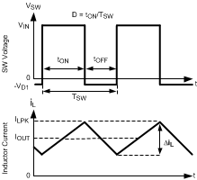
The following operating description of the LMR12015/20 will refer to the Block Diagram and to the waveforms in Figure 22. The LMR12015/20 supplies a regulated output voltage by switching the internal NMOS switch at a constant frequency and varying the duty cycle. A switching cycle begins at the falling edge of the reset pulse generated by the internal oscillator. When this pulse goes low, the output control logic turns on the internal NMOS switch. During this on-time, the SW pin voltage (VSW) swings up to approximately VIN, and the inductor current (iL) increases with a linear slope. The current-sense amplifier measures iL, which generates an output proportional to the switch current typically called the sense signal. The sense signal is summed with the regulator’s corrective ramp and compared to the error amplifier’s output, which is proportional to the difference between the feedback voltage (VFB) and VREF. When the output of the PWM comparator goes high, the switch turns off until the next switching cycle begins. During the switch off-time (tOFF), inductor current discharges through the catch diode D1, which forces the SW pin (VSW) to swing below ground by the forward voltage (VD1) of the catch diode. The regulator loop adjusts the duty cycle (D) to maintain a constant output voltage.
 Figure 22. LMR12015/20 Waveforms of SW Pin Voltage and Inductor Current