SNAS736C June   2017  – April 2019 LMX2595

PRODUCTION DATA.  

  1. Features
  2. Applications
  3. Description
    1.     Device Images
      1.      Simplified Schematic
  4. Revision History
  5. Pin Configuration and Functions
    1.     Pin Functions
  6. Specifications
    1. 6.1 Absolute Maximum Ratings
    2. 6.2 ESD Ratings
    3. 6.3 Recommended Operating Conditions
    4. 6.4 Thermal Information
    5. 6.5 Electrical Characteristics
    6. 6.6 Timing Requirements
    7. 6.7 Typical Characteristics
  7. Detailed Description
    1. 7.1 Overview
    2. 7.2 Functional Block Diagram
    3. 7.3 Feature Description
      1. 7.3.1  Reference Oscillator Input
      2. 7.3.2  Reference Path
        1. 7.3.2.1 OSCin Doubler (OSC_2X)
        2. 7.3.2.2 Pre-R Divider (PLL_R_PRE)
        3. 7.3.2.3 Programmable Multiplier (MULT)
        4. 7.3.2.4 Post-R Divider (PLL_R)
        5. 7.3.2.5 State Machine Clock
      3. 7.3.3  PLL Phase Detector and Charge Pump
      4. 7.3.4  N-Divider and Fractional Circuitry
      5. 7.3.5  MUXout Pin
        1. 7.3.5.1 Lock Detect
        2. 7.3.5.2 Readback
      6. 7.3.6  VCO (Voltage-Controlled Oscillator)
        1. 7.3.6.1 VCO Calibration
        2. 7.3.6.2 Determining the VCO Gain
      7. 7.3.7  Channel Divider
      8. 7.3.8  VCO Doubler
      9. 7.3.9  Output Buffer
      10. 7.3.10 Power-Down Modes
      11. 7.3.11 Phase Synchronization
        1. 7.3.11.1 General Concept
        2. 7.3.11.2 Categories of Applications for SYNC
        3. 7.3.11.3 Procedure for Using SYNC
        4. 7.3.11.4 SYNC Input Pin
      12. 7.3.12 Phase Adjust
      13. 7.3.13 Fine Adjustments for Phase Adjust and Phase SYNC
      14. 7.3.14 Ramping Function
        1. 7.3.14.1 Manual Pin Ramping
          1. 7.3.14.1.1 Manual Pin Ramping Example
        2. 7.3.14.2 Automatic Ramping
          1. 7.3.14.2.1 Automatic Ramping Example (Triangle Wave)
      15. 7.3.15 SYSREF
        1. 7.3.15.1 Programmable Fields
        2. 7.3.15.2 Input and Output Pin Formats
          1. 7.3.15.2.1 Input Format for SYNC and SysRefReq Pins
          2. 7.3.15.2.2 SYSREF Output Format
        3. 7.3.15.3 Examples
        4. 7.3.15.4 SYSREF Procedure
      16. 7.3.16 SysRefReq Pin
    4. 7.4 Device Functional Modes
    5. 7.5 Programming
      1. 7.5.1 Recommended Initial Power-Up Sequence
      2. 7.5.2 Recommended Sequence for Changing Frequencies
      3. 7.5.3 General Programming Requirements
    6. 7.6 Register Maps
      1. 7.6.1  General Registers R0, R1, & R7
        1. Table 25. Field Descriptions
      2. 7.6.2  Input Path Registers
        1. Table 26. Field Descriptions
      3. 7.6.3  Charge Pump Registers (R13, R14)
        1. Table 27. Field Descriptions
      4. 7.6.4  VCO Calibration Registers
        1. Table 28. Field Descriptions
      5. 7.6.5  N Divider, MASH, and Output Registers
        1. Table 29. Field Descriptions
      6. 7.6.6  SYNC and SysRefReq Input Pin Register
        1. Table 30. Field Descriptions
      7. 7.6.7  Lock Detect Registers
        1. Table 31. Field Descriptions
      8. 7.6.8  MASH_RESET
        1. Table 32. Field Descriptions
      9. 7.6.9  SysREF Registers
        1. Table 33. Field Descriptions
      10. 7.6.10 CHANNEL Divider And VCO Doubler Registers
        1. Table 34. Field Descriptions
      11. 7.6.11 Ramping and Calibration Fields
        1. Table 35. Field Descriptions
      12. 7.6.12 Ramping Registers
        1. 7.6.12.1 Ramp Limits
          1. Table 36. Field Descriptions
        2. 7.6.12.2 Ramping Triggers, Burst Mode, and RAMP0_RST
          1. Table 37. Field Descriptions
        3. 7.6.12.3 Ramping Configuration
          1. Table 38. Field Descriptions
      13. 7.6.13 Readback Registers
        1. Table 39. Field Descriptions
  8. Application and Implementation
    1. 8.1 Application Information
      1. 8.1.1 OSCin Configuration
      2. 8.1.2 OSCin Slew Rate
      3. 8.1.3 RF Output Buffer Power Control
      4. 8.1.4 RF Output Buffer Pullup
      5. 8.1.5 Performance Comparison Between 1572 (0x0624) and 3115 (0x0C2B) for Register DBLR_IBIAS_CTRL1 (R25[15:0])
    2. 8.2 Typical Application
      1. 8.2.1 Design Requirements
      2. 8.2.2 Detailed Design Procedure
      3. 8.2.3 Application Curve
  9. Power Supply Recommendations
  10. 10Layout
    1. 10.1 Layout Guidelines
    2. 10.2 Layout Example
  11. 11Device and Documentation Support
    1. 11.1 Device Support
      1. 11.1.1 Third-Party Products Disclaimer
      2. 11.1.2 Development Support
    2. 11.2 Documentation Support
      1. 11.2.1 Related Documentation
    3. 11.3 Receiving Notification of Documentation Updates
    4. 11.4 Community Resources
    5. 11.5 Trademarks
    6. 11.6 Electrostatic Discharge Caution
    7. 11.7 Glossary
  12. 12Mechanical, Packaging, and Orderable Information

Package Options

Mechanical Data (Package|Pins)
Thermal pad, mechanical data (Package|Pins)
Orderable Information

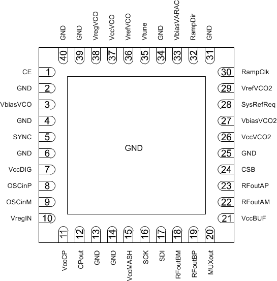
Pin Configuration and Functions

RHA Package
40-Pin VQFN
Top View
LMX2595 po_snas696.gif

Pin Functions

PIN I/O DESCRIPTION
NO. NAME
1 CE Input Chip enable input. Active HIGH powers on the device.
2, 4, 25, 31, 34, 39, 40 GND Ground VCO ground.
3 VbiasVCO Bypass VCO bias. Requires a 10-µF capacitor connected to VCO ground. Place close to pin.
5 SYNC Input Phase synchronization pin. Has programmable threshold.
6, 14 GND Ground Digital ground.
7 VccDIG Supply Digital supply. TI recommends bypassing with decoupling capacitor to digital ground.
8 OSCinP Input Reference input clock (+). High-impedance self-biasing pin. Requires AC-coupling capacitor.
(0.1 µF recommended)
9 OSCinM Input Reference input clock (–). High impedance self-biasing pin. Requires AC-coupling capacitor.
(0.1 µF recommended)
10 VregIN Bypass Input reference path regulator output. Requires a 1-µF capacitor connected to ground. Place close to pin.
11 VccCP Supply Charge pump supply. TI recommends bypassing with decoupling capacitor to charge pump ground.
12 CPout Output Charge pump output. TI recommends connecting C1 of loop filter close to pin.
13 GND Ground Charge pump ground.
15 VccMASH Supply Digital supply. TI recommends bypassing with decoupling capacitor to digital ground.
16 SCK Input SPI clock. High impedance CMOS input. 1.8-V to 3.3-V logic.
17 SDI Input SPI data. High impedance CMOS input. 1.8-V to 3.3-V logic.
18 RFoutBM Output Differential output B (–). Requires a pullup (typically 50-Ω resistor) connected to Vcc as close to the pin as possible. Can be used as an output signal or SYSREF output.
19 RFoutBP Output Differential output B (+). Requires a pullup (typically 50-Ω resistor) connected to Vcc as close to the pin as possible. Can be used as an output signal or SYSREF output.
20 MUXout Output Multiplexed output pin — lock detect, readback, diagnostics, ramp status.
21 VccBUF Supply Output buffer supply. TI recommends bypassing with decoupling capacitor to RFout ground.
22 RFoutAM Output Differential output A (–). Requires connecting a 50-Ω resistor pullup to Vcc as close to the pin as possible.
23 RFoutAP Output Differential output A (+). Requires connecting a 50-Ω resistor pullup to Vcc as close to the pin as possible.
24 CSB Input SPI latch. Chip Select Bar. High-impedance CMOS input. 1.8-V to 3.3-V logic.
26 VccVCO2 Supply VCO supply. TI recommends bypassing with decoupling capacitor to VCO ground.
27 VbiasVCO2 Bypass VCO bias. Requires a 1-µF capacitor connected to VCO ground.
28 SysRefReq Input SYSREF request input for JESD204B support.
29 VrefVCO2 Bypass VCO supply reference. Requires a 10-µF capacitor connected to VCO ground.
30 RampClk Input Input pin for ramping mode that can be used to clock the ramp in manual ramping mode or as a trigger input.
32 RampDir Input Input pin for ramping mode that can be used to change ramp direction in manual ramping mode or as a trigger input.
33 VbiasVARAC Bypass VCO Varactor bias. Requires a 10-µF capacitor connected to VCO ground.
35 Vtune Input VCO tuning voltage input.
36 VrefVCO Bypass VCO supply reference. Requires a 10-µF capacitor connected to VCO ground.
37 VccVCO Supply VCO supply. Recommend bypassing with decoupling capacitor to ground.
38 VregVCO Bypass VCO regulator node. Requires a 1-µF capacitor connected to ground.
DAP GND Ground Die Attached Pad. Used for RFout ground.