SLVSBM9E October 2013 – September 2018 LMZ31520
PRODUCTION DATA.
- 1 Features
- 2 Applications
- 3 Description
- 4 Specifications
- 5 Device Information
- 6 Typical Characteristics (PVIN = VIN = 12 V)
- 7 Typical Characteristics (PVIN = VIN = 5 V)
-
8 Application Information
- 8.1 Adjusting the Output Voltage
- 8.2 Frequency Select
- 8.3 Capacitor Recommendations for the LMZ31520 Power Supply
- 8.4 Transient Response
- 8.5 Application Curves Device configured for FCCM mode of operation, (pin 3 connected to pin 19).
- 8.6 Application Schematics
- 8.7 Custom Design With WEBENCH® Tools
- 8.8 VIN and PVIN Input Voltage
- 8.9 3.3 V PVIN Operation
- 8.10 Power Good (PWRGD)
- 8.11 Slow Start (SS_SEL)
- 8.12 Auto-Skip Eco-mode / Forced Continuous Conduction Mode
- 8.13 Power-Up Characteristics
- 8.14 Pre-Biased Start-Up
- 8.15 Remote Sense
- 8.16 Output On/Off Inhibit (INH)
- 8.17 Overcurrent Protection
- 8.18 Current Limit (ILIM) Adjust
- 8.19 Thermal Shutdown
- 8.20 Layout Considerations
- 8.21 EMI
- 9 Revision History
- 10Device and Documentation Support
- 11Mechanical, Packaging, and Orderable Information
Package Options
Refer to the PDF data sheet for device specific package drawings
Mechanical Data (Package|Pins)
- RLG|72
Thermal pad, mechanical data (Package|Pins)
Orderable Information
8.21 EMI
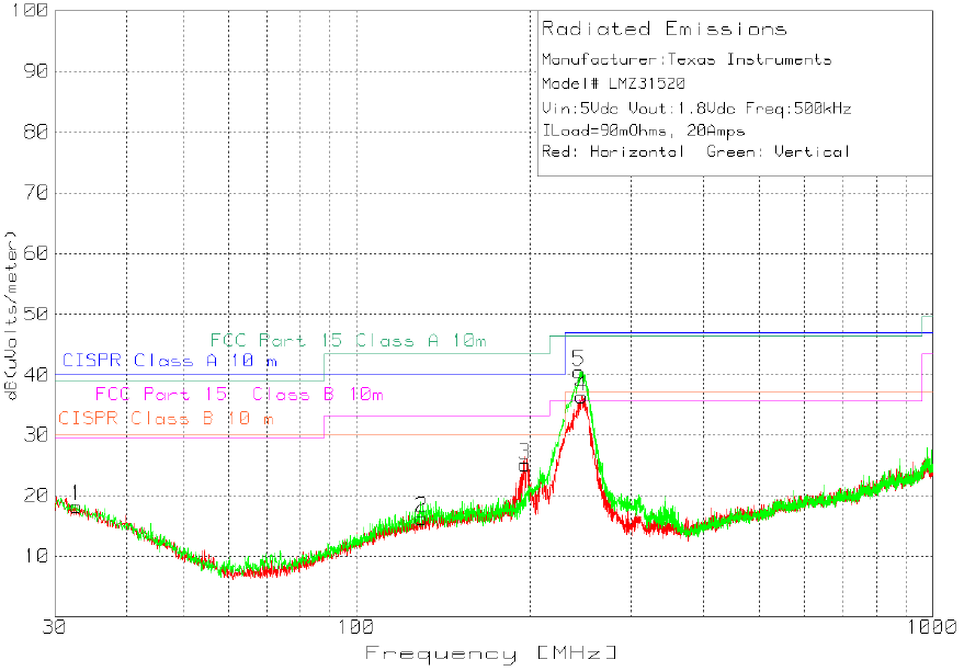
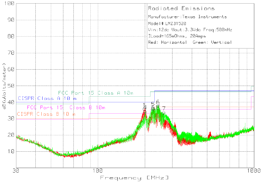
The LMZ31520 is compliant with EN55022 Class A radiated emissions. Figure 31 and Figure 32 show typical examples of radiated emissions plots for the LMZ31520 operating from 5V and 12V respectively. Both graphs include the plots of the antenna in the horizontal and vertical positions.
 Figure 31. Radiated Emissions 5-V Input, 1.8-V Output, 20-A Load (EN55022 Class A)
  Figure 32. Radiated Emissions 12-V Input, 3.3-V Output, 20-A Load (EN55022 Class A)