SLVSBC7E October 2013 – September 2018 LMZ31530
PRODUCTION DATA.
- 1 Features
- 2 Applications
- 3 Description
- 4 Specifications
- 5 Device Information
- 6 Typical Characteristics (PVIN = VIN = 12 V)
- 7 Typical Characteristics (PVIN = VIN = 5 V)
-
8 Application Information
- 8.1 Adjusting the Output Voltage
- 8.2 Frequency Select
- 8.3 Capacitor Recommendations for the LMZ31530 Power Supply
- 8.4 Transient Response
- 8.5 Application Curves
- 8.6 Application Schematics
- 8.7 Custom Design With WEBENCH® Tools
- 8.8 VIN and PVIN Input Voltage
- 8.9 3.3 V PVIN Operation
- 8.10 Power Good (PWRGD)
- 8.11 Slow Start (SS_SEL)
- 8.12 Auto-Skip Eco-mode / Forced Continuous Conduction Mode
- 8.13 Power-Up Characteristics
- 8.14 Pre-Biased Start-Up
- 8.15 Remote Sense
- 8.16 Output On/Off Inhibit (INH)
- 8.17 Overcurrent Protection
- 8.18 Current Limit (ILIM) Adjust
- 8.19 Thermal Shutdown
- 8.20 Layout Considerations
- 8.21 EMI
- 9 Revision History
- 10Device and Documentation Support
- 11Mechanical, Packaging, and Orderable Information
Package Options
Refer to the PDF data sheet for device specific package drawings
Mechanical Data (Package|Pins)
- RLG|72
Thermal pad, mechanical data (Package|Pins)
Orderable Information
8.5 Application Curves
Device configured for FCCM mode of operation, (pin 3 connected to pin 19).
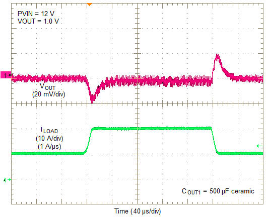
 Figure 13. PVIN = 12V, VOUT = 1.0V, 10A Load Step
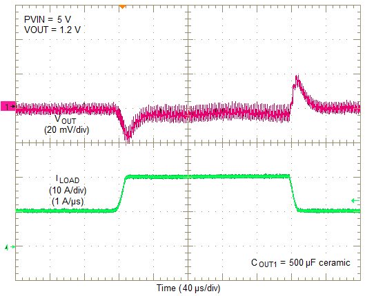
  Figure 15. PVIN = 5V, VOUT = 1.2V, 10A Load Step
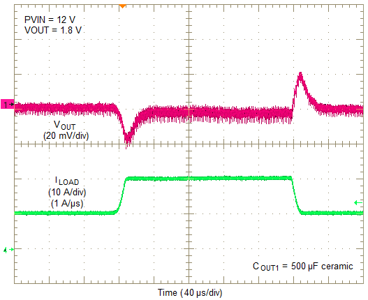
  Figure 14. PVIN = 12V, VOUT = 1.8V, 10A Load Step
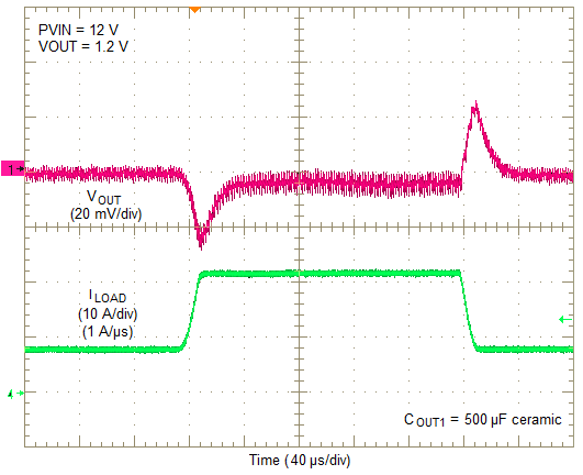
  Figure 16. PVIN = 12V, VOUT = 1.2V, 5A Load Step