SLVSBC7E October 2013 – September 2018 LMZ31530
PRODUCTION DATA.
- 1 Features
- 2 Applications
- 3 Description
- 4 Specifications
- 5 Device Information
- 6 Typical Characteristics (PVIN = VIN = 12 V)
- 7 Typical Characteristics (PVIN = VIN = 5 V)
-
8 Application Information
- 8.1 Adjusting the Output Voltage
- 8.2 Frequency Select
- 8.3 Capacitor Recommendations for the LMZ31530 Power Supply
- 8.4 Transient Response
- 8.5 Application Curves
- 8.6 Application Schematics
- 8.7 Custom Design With WEBENCH® Tools
- 8.8 VIN and PVIN Input Voltage
- 8.9 3.3 V PVIN Operation
- 8.10 Power Good (PWRGD)
- 8.11 Slow Start (SS_SEL)
- 8.12 Auto-Skip Eco-mode / Forced Continuous Conduction Mode
- 8.13 Power-Up Characteristics
- 8.14 Pre-Biased Start-Up
- 8.15 Remote Sense
- 8.16 Output On/Off Inhibit (INH)
- 8.17 Overcurrent Protection
- 8.18 Current Limit (ILIM) Adjust
- 8.19 Thermal Shutdown
- 8.20 Layout Considerations
- 8.21 EMI
- 9 Revision History
- 10Device and Documentation Support
- 11Mechanical, Packaging, and Orderable Information
Package Options
Refer to the PDF data sheet for device specific package drawings
Mechanical Data (Package|Pins)
- RLG|72
Thermal pad, mechanical data (Package|Pins)
Orderable Information
5 Device Information
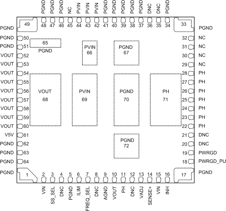
RLG PACKAGE
(TOP VIEW)

Pin Functions
| TERMINAL | DESCRIPTION | |
|---|---|---|
| NAME | NO. | |
| AGND | 9 | This pin is connected internally to the power ground of the device. This pin should only be used as the zero volt ground reference for connecting the voltage setting resistor (RSET). Do not connect AGND to PGND. See Layout Recommendations. |
| DNC | 4 | Do Not Connect. Do not connect these pins to AGND, to another DNC pin, or to any other voltage. These pins are connected to internal circuitry. Each pin must be soldered to an isolated pad. |
| 8 | ||
| 12 | ||
| 20 | ||
| 21 | ||
| 35 | ||
| 36 | ||
| FREQ_SEL | 7 | Frequency Select pin. Leave this pin open (floating) to select 500 kHz (typ) operating frequency. Connect this pin to V5V pin to select 850 kHz (typ) operating frequency. Connect a 66 kΩ resistor between this pin and PGND to select 300 kHz (typ) operating frequency. See Table 2 for more info. |
| ILIM | 6 | Current limit setting pin. Connecting a resistor between this pin and PGND sets the current limit. When left open, refer to the Electrical Characterization table for current limit value. |
| INH | 16 | Inhibit pin. Use an open drain or open collector logic device to ground this pin to control the INH function. |
| NC | 29 | Not Connected. These pins are internally isolated from any signal and all other pins. Each pin must be soldered to a pad on the PCB. These pins can be left isolated, connected to one another, or connected to any signal on the PCB. |
| 30 | ||
| 31 | ||
| 32 | ||
| 45 | ||
| PGND | 1 | This is the return current path for the power stage of the device. Connect these pins to the load and to the bypass capacitors associated with VIN and VOUT. Pads 65, 67, 70, and 72 should be connected to PCB ground planes using multiple vias for good thermal performance. Not all pins are connected together internally. All pins must be connected together externally with a copper plane or pour directly under the device. |
| 5 | ||
| 17 | ||
| 33 | ||
| 34 | ||
| 37 | ||
| 38 | ||
| 39 | ||
| 40 | ||
| 41 | ||
| 46 | ||
| 47 | ||
| 48 | ||
| 49 | ||
| 50 | ||
| 51 | ||
| 62 | ||
| 63 | ||
| 64 | ||
| 65 | ||
| 67 | ||
| 70 | ||
| 72 | ||
| PH | 11 | Phase switch node. Do not place any external component on these pins or tie them to a pin of another function. Connect these pins using a copper area beneath pad 71. |
| 22 | ||
| 23 | ||
| 24 | ||
| 25 | ||
| 26 | ||
| 27 | ||
| 28 | ||
| 71 | ||
| PVIN | 42 | Input switching voltage pin. This pin supplies voltage to the power switches of the converter. |
| 43 | ||
| 44 | ||
| 66 | ||
| 69 | ||
| PWRGD | 19 | Power Good flag pin. This open drain output asserts low if the output voltage is more than approximately ±6% out of regulation. |
| PWRGD_PU | 18 | Power Good pull-up pin. This pin is connected to a 100kΩ resistor which is tied to the PWRGD pin internally. Connect this pin to V5V or to any voltage between 1.3V and 6.5V. |
| SENSE+ | 14 | Remote sense connection. Connect this pin to VOUT at the load for improved regulation. This pin must be connected to VOUT at the load, or at the module pins. |
| SS_SEL | 3 | Slow-start select pin. Connect a resistor between this pin and PWRGD (or PGND) to select the slow-start time. See the SS_SEL section of the datasheet for slow-start times and corresponding resistor values. Connect the SS_SEL pin to PGND to select Auto-skip Eco-mode or to the PWRGD pin (pin 19) to select FCCM. |
| V5V | 61 | 5V regulator pin. This regulator supplies the internal circuitry. |
| VADJ | 13 | Output voltage adjust pin. Connecting a resistor between this pin and AGND sets the output voltage. |
| VIN | 2 | Input bias voltage pins. Supplies the control circuitry of the power converter. |
| 15 | ||
| VOUT | 10 | Output voltage. These pins are connected to the internal output inductor. Connect these pins to the output load and connect external bypass capacitors between these pins and PGND. |
| 52 | ||
| 53 | ||
| 54 | ||
| 55 | ||
| 56 | ||
| 57 | ||
| 58 | ||
| 59 | ||
| 60 | ||
| 68 | ||
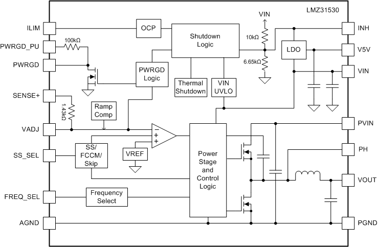
5.1 Functional Block Diagram
