SLVSBC7E October 2013 – September 2018 LMZ31530
PRODUCTION DATA.
- 1 Features
- 2 Applications
- 3 Description
- 4 Specifications
- 5 Device Information
- 6 Typical Characteristics (PVIN = VIN = 12 V)
- 7 Typical Characteristics (PVIN = VIN = 5 V)
-
8 Application Information
- 8.1 Adjusting the Output Voltage
- 8.2 Frequency Select
- 8.3 Capacitor Recommendations for the LMZ31530 Power Supply
- 8.4 Transient Response
- 8.5 Application Curves
- 8.6 Application Schematics
- 8.7 Custom Design With WEBENCH® Tools
- 8.8 VIN and PVIN Input Voltage
- 8.9 3.3 V PVIN Operation
- 8.10 Power Good (PWRGD)
- 8.11 Slow Start (SS_SEL)
- 8.12 Auto-Skip Eco-mode / Forced Continuous Conduction Mode
- 8.13 Power-Up Characteristics
- 8.14 Pre-Biased Start-Up
- 8.15 Remote Sense
- 8.16 Output On/Off Inhibit (INH)
- 8.17 Overcurrent Protection
- 8.18 Current Limit (ILIM) Adjust
- 8.19 Thermal Shutdown
- 8.20 Layout Considerations
- 8.21 EMI
- 9 Revision History
- 10Device and Documentation Support
- 11Mechanical, Packaging, and Orderable Information
Package Options
Refer to the PDF data sheet for device specific package drawings
Mechanical Data (Package|Pins)
- RLG|72
Thermal pad, mechanical data (Package|Pins)
Orderable Information
8.20 Layout Considerations
To achieve optimal electrical and thermal performance, an optimized PCB layout is required. Figure 28 thru Figure 33, shows a typical PCB layout. Some considerations for an optimized layout are:
- Use large copper areas for power planes (PVIN, VOUT, and PGND) to minimize conduction loss and thermal stress.
- Place ceramic input and output capacitors close to the device pins to minimize high frequency noise.
- Locate additional output capacitors between the ceramic capacitor and the load.
- Keep AGND and PGND separate from one another. AGND should only be used as the return for RSET.
- Place RSET, RFREQ, and RSS as close as possible to their respective pins.
- Use multiple vias to connect the power planes to internal layers.
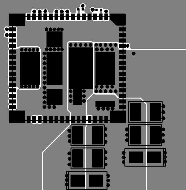 Figure 28. Typical Top Layer Layout
 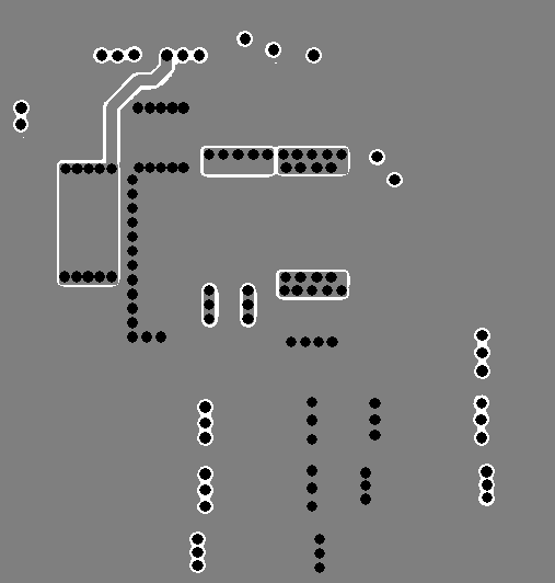 Figure 30. Typical Layer 3 Layout
 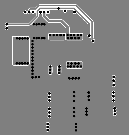 Figure 32. Typical Layer 5 Layout
 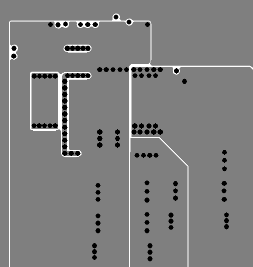 Figure 29. Typical Layer 2 Layout
 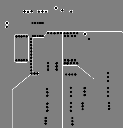 Figure 31. Typical Layer 4 Layout
 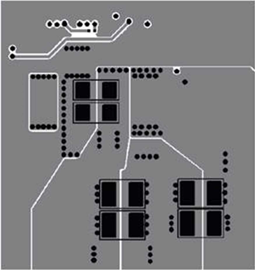 Figure 33. Typical Bottom Layer Layout