SBOS701D December 2015 – August 2021 OPA191 , OPA2191 , OPA4191
PRODUCTION DATA
- 1 Features
- 2 Applications
- 3 Description
- 4 Revision History
- 5 Pin Configuration and Functions
-
6 Specifications
- 6.1 Absolute Maximum Ratings
- 6.2 ESD Ratings
- 6.3 Recommended Operating Conditions
- 6.4 Thermal Information: OPA191
- 6.5 Thermal Information: OPA2191
- 6.6 Thermal Information: OPA4191
- 6.7 Electrical Characteristics: VS = ±4 V to ±18 V (VS = 8 V to 36 V)
- 6.8 Electrical Characteristics: VS = ±2.25 V to ±4 V (VS = 4.5 V to 8 V)
- 6.9 Typical Characteristics
- 7 Parameter Measurement Information
- 8 Detailed Description
- 9 Application and Implementation
- 10Power Supply Recommendations
- 11Layout
- 12Device and Documentation Support
- 13Mechanical, Packaging, and Orderable Information
Package Options
Mechanical Data (Package|Pins)
Thermal pad, mechanical data (Package|Pins)
Orderable Information
9.2.1.2 Detailed Design Procedure
The transfer function of the circuit in Figure 9-1 is given in Equation 2

The load current (ILOAD) produces a voltage drop across the shunt resistor (RSHUNT). The load current is set from 0 A to 1 A. To keep the shunt voltage below 100 mV at maximum load current, the largest shunt resistor is defined using Equation 3.

Using Equation 3, RSHUNT is calculated to be 100 mΩ. The voltage drop produced by ILOAD and RSHUNT is amplified by the OPA191 to produce an output voltage of 0 V to 4.9 V. The gain needed by the OPA191 to produce the necessary output voltage is calculated using Equation 4:
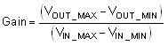
Using Equation 4, the required gain is calculated to be 49 V/V, which is set with resistors RF and RG. Equation 5 is used to size the resistors, RF and RG, to set the gain of the OPA191 to 49 V/V.

Choosing RF as 360 kΩ, RG is calculated to be 7.5 kΩ. RF and RG were chosen as 360 kΩ and 7.5 kΩ because they are standard value resistors that create a 49:1 ratio. Other resistors that create a 49:1 ratio can also be used. Figure 2 shows the measured transfer function of the circuit shown in Figure 9-1.