SBOS637D October   2016  – June 2019 OPA2325 , OPA325 , OPA4325

PRODUCTION DATA.  

  1. Features
  2. Applications
    1.     Offset Voltage vs Input Common-Mode Voltage
  3. Description
    1.     The OPAx325 as an ADC Driver Amplifier
  4. Revision History
  5. Pin Configuration and Functions
    1.     Pin Functions: OPA325
    2.     Pin Functions: OPA2325
    3.     Pin Functions: OPA4325
  6. Specifications
    1. 6.1 Absolute Maximum Ratings
    2. 6.2 ESD Ratings
    3. 6.3 Recommended Operating Conditions
    4. 6.4 Thermal Information: OPA325
    5. 6.5 Thermal Information: OPA2325
    6. 6.6 Thermal Information: OPA4325
    7. 6.7 Electrical Characteristics: VS = 2.2 V to 5.5 V or ±1.1 V to ±2.75 V
    8. 6.8 Typical Characteristics
  7. Detailed Description
    1. 7.1 Overview
    2. 7.2 Functional Block Diagram
    3. 7.3 Feature Description
      1. 7.3.1 Zero-Crossover Input Stage
      2. 7.3.2 Low Input Offset Voltage
      3. 7.3.3 Input and ESD Protection
    4. 7.4 Device Functional Modes
  8. Application and Implementation
    1. 8.1 Application Information
      1. 8.1.1 Operating Characteristics
      2. 8.1.2 Basic Amplifier Configurations
      3. 8.1.3 Driving an Analog-to-Digital Converter
    2. 8.2 Typical Application
      1. 8.2.1 Design Requirements
      2. 8.2.2 Detailed Design Procedure
      3. 8.2.3 Application Curves
  9. Power Supply Recommendations
  10. 10Layout
    1. 10.1 Layout Guidelines
    2. 10.2 Layout Example
  11. 11Device and Documentation Support
    1. 11.1 Documentation Support
      1. 11.1.1 Related Documentation
    2. 11.2 Related Links
    3. 11.3 Receiving Notification of Documentation Updates
    4. 11.4 Community Resources
    5. 11.5 Trademarks
    6. 11.6 Electrostatic Discharge Caution
    7. 11.7 Glossary
  12. 12Mechanical, Packaging, and Orderable Information

Package Options

Mechanical Data (Package|Pins)
Thermal pad, mechanical data (Package|Pins)
Orderable Information

Basic Amplifier Configurations

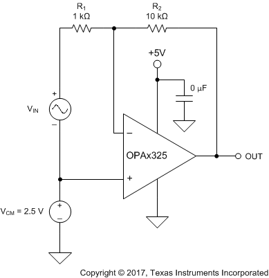
The OPAx325 are unity-gain stable. The devices do not exhibit output phase inversion when the input is overdriven. A typical single-supply connection is shown in Figure 44. The OPAx325 are configured as a basic inverting amplifier with a gain of –10 V/V. This single-supply connection has an output centered on the common-mode voltage, VCM. For the circuit shown, this voltage is 2.5 V, but can be any value within the common-mode input voltage range.
OPA325 OPA2325 OPA4325 s001_SBOS637.gifFigure 44. Basic Single-Supply Connection