SBOS637D October   2016  – June 2019 OPA2325 , OPA325 , OPA4325

PRODUCTION DATA.  

  1. Features
  2. Applications
    1.     Offset Voltage vs Input Common-Mode Voltage
  3. Description
    1.     The OPAx325 as an ADC Driver Amplifier
  4. Revision History
  5. Pin Configuration and Functions
    1.     Pin Functions: OPA325
    2.     Pin Functions: OPA2325
    3.     Pin Functions: OPA4325
  6. Specifications
    1. 6.1 Absolute Maximum Ratings
    2. 6.2 ESD Ratings
    3. 6.3 Recommended Operating Conditions
    4. 6.4 Thermal Information: OPA325
    5. 6.5 Thermal Information: OPA2325
    6. 6.6 Thermal Information: OPA4325
    7. 6.7 Electrical Characteristics: VS = 2.2 V to 5.5 V or ±1.1 V to ±2.75 V
    8. 6.8 Typical Characteristics
  7. Detailed Description
    1. 7.1 Overview
    2. 7.2 Functional Block Diagram
    3. 7.3 Feature Description
      1. 7.3.1 Zero-Crossover Input Stage
      2. 7.3.2 Low Input Offset Voltage
      3. 7.3.3 Input and ESD Protection
    4. 7.4 Device Functional Modes
  8. Application and Implementation
    1. 8.1 Application Information
      1. 8.1.1 Operating Characteristics
      2. 8.1.2 Basic Amplifier Configurations
      3. 8.1.3 Driving an Analog-to-Digital Converter
    2. 8.2 Typical Application
      1. 8.2.1 Design Requirements
      2. 8.2.2 Detailed Design Procedure
      3. 8.2.3 Application Curves
  9. Power Supply Recommendations
  10. 10Layout
    1. 10.1 Layout Guidelines
    2. 10.2 Layout Example
  11. 11Device and Documentation Support
    1. 11.1 Documentation Support
      1. 11.1.1 Related Documentation
    2. 11.2 Related Links
    3. 11.3 Receiving Notification of Documentation Updates
    4. 11.4 Community Resources
    5. 11.5 Trademarks
    6. 11.6 Electrostatic Discharge Caution
    7. 11.7 Glossary
  12. 12Mechanical, Packaging, and Orderable Information

Package Options

Mechanical Data (Package|Pins)
Thermal pad, mechanical data (Package|Pins)
Orderable Information

Typical Application

Operational amplifiers are commonly used as unity-gain buffers. Figure 46 shows the schematic for an amplifier configured as a unity-gain buffer. If the input signal range to the amplifier is very close to the rails or includes the rails, a rail-to-rail amplifier must be used. However, regular rail-to-rail amplifiers introduce significant distortion to the signal. This design compares the distortion introduced by a typical CMOS input amplifier with that of the OPAx325 (a zero-crossover amplifier).
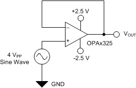
OPA325 OPA2325 OPA4325 G-1-bos637.gifFigure 46. The OPAx325 Configured as a Unity-Gain Buffer Amplifier