SBOS637D October 2016 – June 2019 OPA2325 , OPA325 , OPA4325
PRODUCTION DATA.
- 1 Features
- 2 Applications
- 3 Description
- 4 Revision History
- 5 Pin Configuration and Functions
- 6 Specifications
- 7 Detailed Description
- 8 Application and Implementation
- 9 Power Supply Recommendations
- 10Layout
- 11Device and Documentation Support
- 12Mechanical, Packaging, and Orderable Information
Package Options
Mechanical Data (Package|Pins)
Thermal pad, mechanical data (Package|Pins)
Orderable Information
7.3.1 Zero-Crossover Input Stage
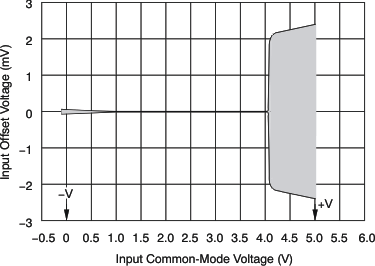
Traditional complementary metal-oxide semiconductor (CMOS) rail-to-rail input amplifiers use a complementary input stage: an N-channel input differential pair in parallel with a P-channel differential pair. This configuration results in sudden change in offset voltage when the input stage transitions from the p-channel metal-oxide-semiconductor field effect transistor (PMOS) to the n-type field effect transistor (NMOS), or vice-versa, as shown in Figure 40. This transition results in significant degradation of CMRR and PSRR performance of the amplifier.
.
 Figure 40. Input Common-Mode Voltage vs Input Offset Voltage
(Traditional Rail-to-Rail Input CMOS Amplifiers)
The OPAx325 series of amplifiers includes an internal charge pump that powers the amplifier input stage with an internal supply rail that is higher than the external power supply. The internal supply rail allows a single differential pair to operate and to be linear across the entire input common-mode voltage range, thus eliminating crossover distortion. Rail-to-rail amplifiers that use this technique to eliminate crossover distortion are called zero-crossover amplifiers.
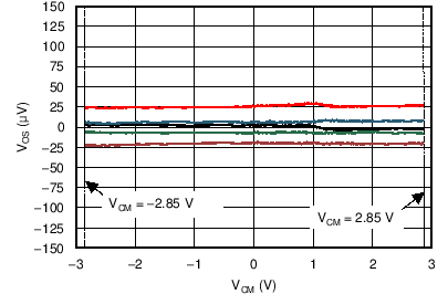
The single differential pair combined with the charge pump allows the OPAx325 to provide superior CMRR across the entire common-mode input range, which extends 100 mV beyond both power-supply rails. Figure 41 shows the input offset voltage versus input common-mode voltage plot for the OPAx325. Note that unlike traditional rail-to-rail CMOS amplifiers, there is no transition region for the OPAx325.
 Figure 41. Offset Voltage vs Common-Mode Voltage (Zero-Crossover)