SCPS123F March 2005 – January 2015 PCF8575C
PRODUCTION DATA.
- 1 Features
- 2 Applications
- 3 Description
- 4 Revision History
- 5 Pin Configuration
- 6 Specifications
- 7 Parameter Measurement Information
- 8 Detailed Description
- 9 Application and Implementation
- 10Power Supply Recommendations
- 11Layout
- 12Device and Documentation Support
- 13Mechanical, Packaging, and Orderable Information
Package Options
Mechanical Data (Package|Pins)
Thermal pad, mechanical data (Package|Pins)
- RGE|24
Orderable Information
9 Application and Implementation
NOTE
Information in the following applications sections is not part of the TI component specification, and TI does not warrant its accuracy or completeness. TI’s customers are responsible for determining suitability of components for their purposes. Customers should validate and test their design implementation to confirm system functionality.
9.1 Application Information
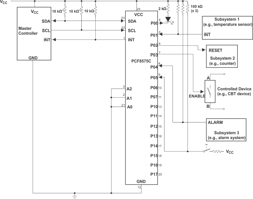
Figure 15 shows an application in which the PCF8575C can be used.
9.2 Typical Application
9.2.1 Design Requirements
9.2.1.1 Minimizing ICC When I/Os Control LEDs
When the I/Os are used to control LEDs, normally they are connected to VCC through a resistor as shown in Figure 15. For a P-port configured as an input, ICC increases as VI becomes lower than VCC. The LED is a diode, with threshold voltage VT, and when a P-port is configured as an input the LED will be off but VI is a VT drop below VCC.
For battery-powered applications, it is essential that the voltage of P-ports controlling LEDs is greater than or equal to VCC when the P-ports are configured as input to minimize current consumption. Figure 16 shows a high-value resistor in parallel with the LED. Figure 17 shows VCC less than the LED supply voltage by at least VT. Both of these methods maintain the I/O VI at or above VCC and prevents additional supply current consumption when the P-port is configured as an input and the LED is off.
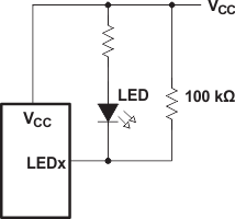 Figure 16. High-Value Resistor in Parallel With LED
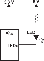 Figure 17. Device Supplied by a Lower Voltage
9.2.2 Detailed Design Procedure
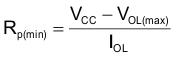
The pull-up resistors, RP, for the SCL and SDA lines need to be selected appropriately and take into consideration the total capacitance of all slaves on the I2C bus. The minimum pull-up resistance is a function of VCC, VOL,(max), and IOL:
The maximum pull-up resistance is a function of the maximum rise time, tr (300 ns for fast-mode operation, fSCL = 400 kHz) and bus capacitance, Cb:
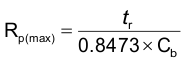
The maximum bus capacitance for an I2C bus must not exceed 400 pF for standard-mode or fast-mode operation. The bus capacitance can be approximated by adding the capacitance of the TCA9534, Ci for SCL or Cio for SDA, the capacitance of wires/connections/traces, and the capacitance of additional slaves on the bus.
9.2.3 Application Curves
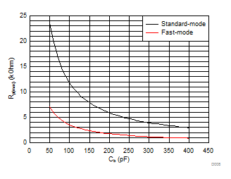
| Standard-mode (fSCL= 100 kHz, tr = 1 µs) |
Fast-mode (fSCL= 400 kHz, tr= 300 ns) |
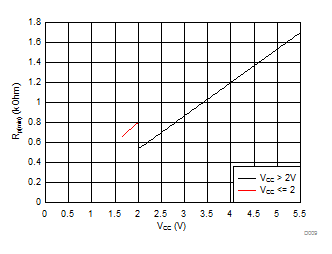
| VOL = 0.2*VCC, IOL = 2 mA when VCC ≤ 2 V | ||
| VOL = 0.4 V, IOL = 3 mA when VCC > 2 V | ||