SCPS123F March 2005 – January 2015 PCF8575C
PRODUCTION DATA.
- 1 Features
- 2 Applications
- 3 Description
- 4 Revision History
- 5 Pin Configuration
- 6 Specifications
- 7 Parameter Measurement Information
- 8 Detailed Description
- 9 Application and Implementation
- 10Power Supply Recommendations
- 11Layout
- 12Device and Documentation Support
- 13Mechanical, Packaging, and Orderable Information
Package Options
Mechanical Data (Package|Pins)
Thermal pad, mechanical data (Package|Pins)
- RGE|24
Orderable Information
8 Detailed Description
8.1 Overview
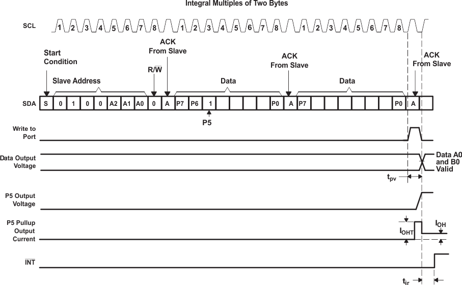
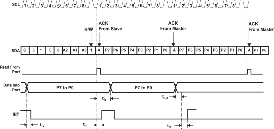
The PCF8575C provides an open-drain interrupt (INT) output, which can be connected to the interrupt input of a microcontroller. An interrupt is generated by any rising or falling edge of the port inputs in the input mode. After time (tiv), the signal INT is valid. Resetting and reactivating the interrupt circuit is achieved when data on the port is changed to the original setting, or data is read from or written to the port that generated the interrupt. Resetting occurs in the read mode at the acknowledge (ACK) bit after the rising edge of the SCL signal or in the write mode at the ACK bit after the falling edge of the SCL signal. Interrupts that occur during the ACK clock pulse can be lost (or be very short), due to the resetting of the interrupt during this pulse. Each change of the I/Os after resetting is detected and is transmitted as INT. Reading from or writing to another device does not affect the interrupt circuit.
By sending an interrupt signal on this line, the remote I/O can inform the microcontroller if there is incoming data on its ports, without having to communicate via the I2C bus. Thus, the PCF8575C can remain a simple slave device.
Every data transmission to or from the PCF8575C must consist of an even number of bytes. The first data byte in every pair refers to port 0 (P07–P00), and the second data byte in every pair refers to port 1 (P17–P10). To write to the ports (output mode), the master first addresses the slave device, setting the last bit of the byte containing the slave address to logic 0. The PCF8575C acknowledges and the master sends the first data byte for P07–P00. After the first data byte is acknowledged by the PCF8575C, the second data byte (P17–P10) is sent by the master. Once again, the PCF8575C acknowledges the receipt of the data, after which this 16-bit data is presented on the port lines.
The number of data bytes that can be sent successively is not limited. After every two bytes, the previous data is overwritten. When the PCF8575C receives the pairs of data bytes, the first byte is referred to as P07–P00 and the second byte as P17–P10. The third byte is referred to as P07–P00, the fourth byte as P17–P10, and so on.
Before reading from the PCF8575C, all ports desired as input should be set to logic 1. To read from the ports (input mode), the master first addresses the slave device, setting the last bit of the byte containing the slave address to logic 1. The data bytes that follow on the SDA are the values on the ports. If the data on the input port changes faster than the master can read, this data may be lost.
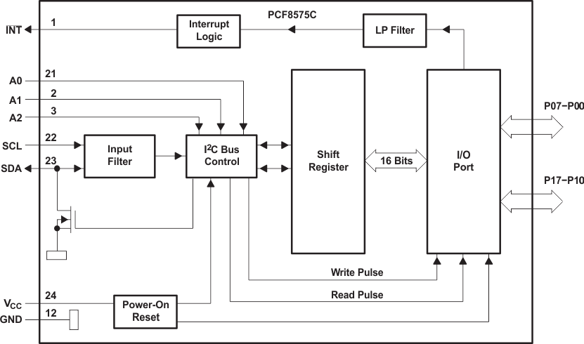
When power is applied to VCC, an internal power-on reset holds the PCF8575C in a reset state until VCC has reached VPOR. At that time, the reset condition is released, and the device I2C-bus state machine initializes the bus to its default state.
The hardware pins (A0, A1, and A2) are used to program and vary the fixed I2C address, and allow up to eight devices to share the same I2C bus or SMBus. The fixed I2C address of the PCF8575C is the same as the PCF8575, PCF8574, PCA9535, and PCA9555, allowing up to eight of these devices, in any combination, to share the same I2C bus or SMBus.
8.2 Functional Block Diagram
8.2.1 Simplified Block Diagram of Device
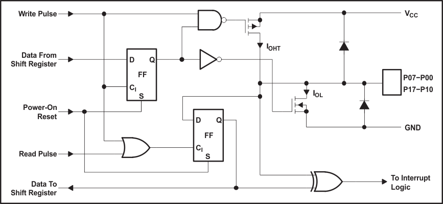
8.2.2 Simplified Schematic Diagram of Each P-Port Input/Output
8.3 Feature Description
8.3.1 I2C Interface
The bidirectional I2C bus consists of the serial clock (SCL) and serial data (SDA) lines. Both lines must be connected to a positive supply via a pullup resistor when connected to the output stages of a device. Data transfer may be initiated only when the bus is not busy.
I2C communication with this device is initiated by a master sending a start condition, a high-to-low transition on the SDA input/output while the SCL input is high (see Figure 10). After the start condition, the device address byte is sent, MSB first, including the data direction bit (R/W). This device does not respond to the general call address. After receiving the valid address byte, this device responds with an ACK, a low on the SDA input/output during the high of the ACK-related clock pulse. The address inputs (A2–A0) of the slave device must not be changed between the start and the stop conditions.
The data byte follows the address ACK. If the R/W bit is high, the data from this device are the values read from the P port. If the R/W bit is low, the data are from the master, to be output to the P port. The data byte is followed by an ACK sent from this device. If other data bytes are sent from the master, following the ACK, they are ignored by this device. Data are output only if complete bytes are received and acknowledged. The output data is valid at time (tpv) after the low-to-high transition of SCL, during the clock cycle for the ACK.
On the I2C bus, only one data bit is transferred during each clock pulse. The data on the SDA line must remain stable during the high pulse of the clock period, as changes in the data line at this time are interpreted as control commands (start or stop) (see Figure 11).
A stop condition, a low-to-high transition on the SDA input/output while the SCL input is high, is sent by the master (see Figure 10).
The number of data bytes transferred between the start and the stop conditions from transmitter to receiver is not limited. Each byte of eight bits is followed by one ACK bit. The transmitter must release the SDA line before the receiver can send an ACK bit.
A slave receiver that is addressed must generate an ACK after the reception of each byte. Also, a master must generate an ACK after the reception of each byte that has been clocked out of the slave transmitter. The device that acknowledges has to pull down the SDA line during the ACK clock pulse so that the SDA line is stable low during the high pulse of the ACK-related clock period (see Figure 12). Setup and hold times must be taken into account.
A master receiver must signal an end of data to the transmitter by not generating an acknowledge (NACK) after the last byte that has been clocked out of the slave. This is done by the master receiver by holding the SDA line high. In this event, the transmitter must release the data line to enable the master to generate a stop condition.
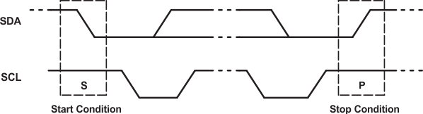 Figure 10. Definition of Start and Stop Conditions
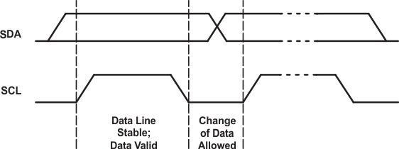 Figure 11. Bit Transfer
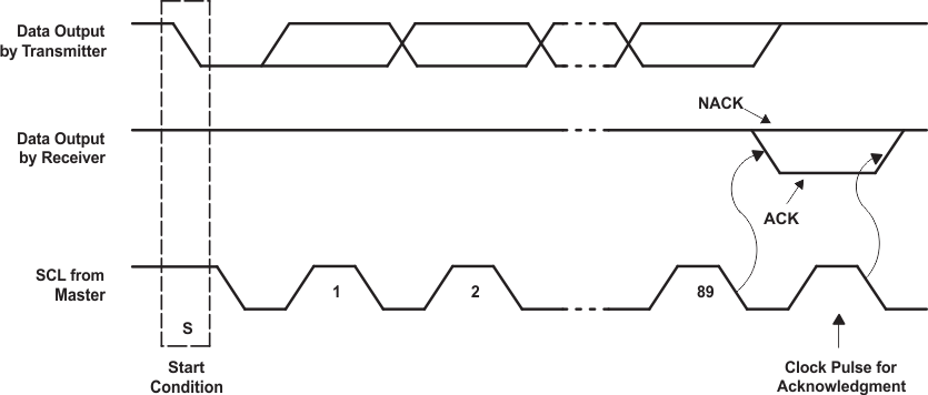 Figure 12. Acknowledgment on I2C Bus
8.3.2 Interface Definition
| BYTE | BIT | |||||||
|---|---|---|---|---|---|---|---|---|
| 7 (MSB) | 6 | 5 | 4 | 3 | 2 | 1 | 0 (LSB) | |
| I2C slave address | L | H | L | L | A2 | A1 | A0 | R/W |
| P0x I/O data bus | P07 | P06 | P05 | P04 | P03 | P02 | P01 | P00 |
| P1x I/O data bus | P17 | P16 | P15 | P14 | P13 | P12 | P11 | P10 |
8.3.3 Address Reference
| INPUTS | I2C BUS SLAVE 8-BIT READ ADDRESS | I2C BUS SLAVE 8-BIT WRITE ADDRESS | ||
|---|---|---|---|---|
| A2 | A1 | A0 | ||
| L | L | L | 65 (decimal), 41 (hexadecimal) | 64 (decimal), 40 (hexadecimal) |
| L | L | H | 67 (decimal), 43 (hexadecimal) | 66 (decimal), 42 (hexadecimal) |
| L | H | L | 69 (decimal), 45 (hexadecimal) | 68 (decimal), 44 (hexadecimal) |
| L | H | H | 71 (decimal), 47 (hexadecimal) | 70 (decimal), 46 (hexadecimal) |
| H | L | L | 73 (decimal), 49 (hexadecimal) | 72 (decimal), 48 (hexadecimal) |
| H | L | H | 75 (decimal), 4B (hexadecimal) | 74 (decimal), 4A (hexadecimal) |
| H | H | L | 77 (decimal), 4D (hexadecimal) | 76 (decimal), 4C (hexadecimal) |
| H | H | H | 79 (decimal), 4F (hexadecimal) | 78 (decimal), 4E (hexadecimal) |