SCPS123F March 2005 – January 2015 PCF8575C
PRODUCTION DATA.
- 1 Features
- 2 Applications
- 3 Description
- 4 Revision History
- 5 Pin Configuration
- 6 Specifications
- 7 Parameter Measurement Information
- 8 Detailed Description
- 9 Application and Implementation
- 10Power Supply Recommendations
- 11Layout
- 12Device and Documentation Support
- 13Mechanical, Packaging, and Orderable Information
Package Options
Mechanical Data (Package|Pins)
Thermal pad, mechanical data (Package|Pins)
- RGE|24
Orderable Information
10 Power Supply Recommendations
10.1 Power-On Reset Requirements
In the event of a glitch or data corruption, PCF8575C can be reset to its default conditions by using the power-on reset feature. Power-on reset requires that the device go through a power cycle to be completely reset. This reset also happens when the device is powered on for the first time in an application.
The two types of power-on reset are shown in Figure 20 and Figure 21.
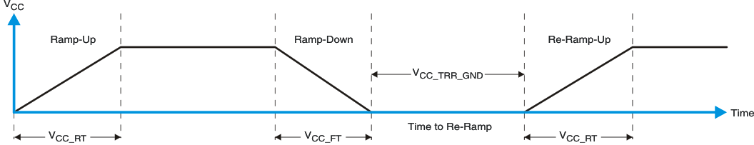 Figure 20. VCC is Lowered Below 0.2 V or 0 V and Then Ramped Up to VCC
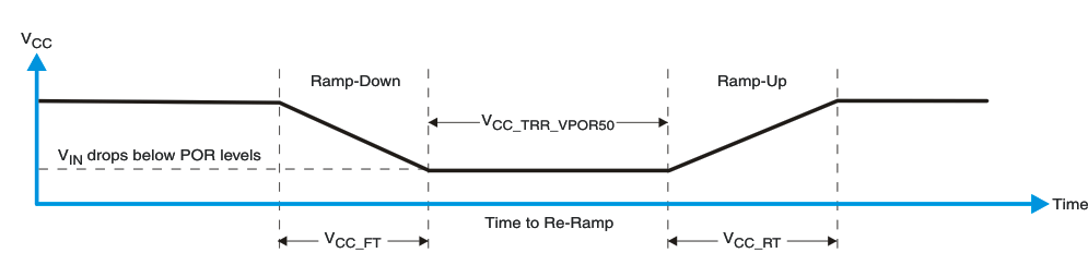 Figure 21. VCC is Lowered Below the POR Threshold, Then Ramped Back Up to VCC
Table 1 specifies the performance of the power-on reset feature for PCF8575C for both types of power-on reset.
Table 1. RECOMMENDED SUPPLY SEQUENCING AND RAMP RATES(1)
| PARAMETER | MIN | TYP | MAX | UNIT | ||
|---|---|---|---|---|---|---|
| VCC_FT | Fall rate | See Figure 20 | 1 | 100 | ms | |
| VCC_RT | Rise rate | See Figure 20 | 0.01 | 100 | ms | |
| VCC_TRR_GND | Time to re-ramp (when VCC drops to GND) | See Figure 20 | 0.001 | ms | ||
| VCC_TRR_POR50 | Time to re-ramp (when VCC drops to VPOR_MIN – 50 mV) | See Figure 21 | 0.001 | ms | ||
| VCC_GH | Level that VCCP can glitch down to, but not cause a functional disruption when VCCX_GW = 1 μs | See Figure 22 | 1.2 | V | ||
| VCC_GW | Glitch width that will not cause a functional disruption when VCCX_GH = 0.5 × VCCx | See Figure 22 | μs | |||
| VPORF | Voltage trip point of POR on falling VCC | 0.767 | 1.144 | V | ||
| VPORR | Voltage trip point of POR on fising VCC | 1.033 | 1.428 | V | ||
Glitches in the power supply can also affect the power-on reset performance of this device. The glitch width (VCC_GW) and height (VCC_GH) are dependent on each other. The bypass capacitance, source impedance, and device impedance are factors that affect power-on reset performance. Figure 22 and Table 1 provide more information on how to measure these specifications.
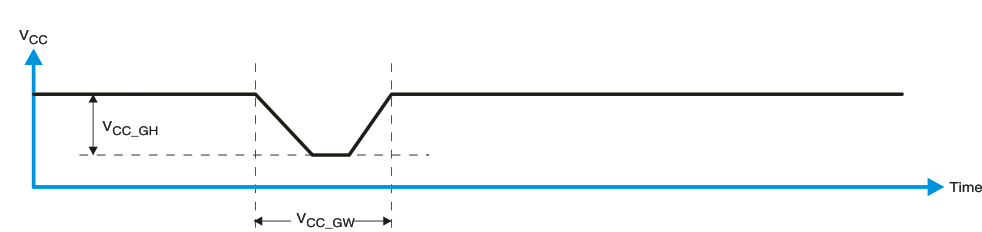 Figure 22. Glitch Width and Glitch Height
VPOR is critical to the power-on reset. VPOR is the voltage level at which the reset condition is released and all the registers and the I2C/SMBus state machine are initialized to their default states. The value of VPOR differs based on the VCC being lowered to or from 0. Figure 23 and Table 1 provide more details on this specification.
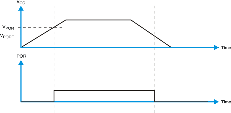 Figure 23. VPOR