SCPS123F March 2005 – January 2015 PCF8575C
PRODUCTION DATA.
- 1 Features
- 2 Applications
- 3 Description
- 4 Revision History
- 5 Pin Configuration
- 6 Specifications
- 7 Parameter Measurement Information
- 8 Detailed Description
- 9 Application and Implementation
- 10Power Supply Recommendations
- 11Layout
- 12Device and Documentation Support
- 13Mechanical, Packaging, and Orderable Information
Package Options
Mechanical Data (Package|Pins)
Thermal pad, mechanical data (Package|Pins)
- RGE|24
Orderable Information
5 Pin Configuration
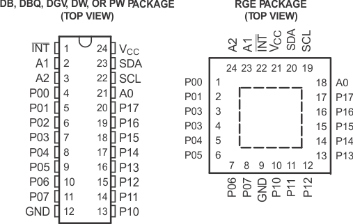
Pin Functions
| PIN | TYPE | DESCRIPTION | ||
|---|---|---|---|---|
| NAME | NO. | |||
| DB, DBQ, DGV, DW, AND PW |
RGE | |||
| INT | 1 | 22 | I | Interrupt output. Connect to VCC through a pullup resistor. |
| A1 | 2 | 23 | I | Address input 1. Connect directly to VCC or ground. Pullup resistors are not needed. |
| A2 | 3 | 24 | I | Address input 2. Connect directly to VCC or ground. Pullup resistors are not needed. |
| P00 | 4 | 1 | I/O | P-port input/output. Open-drain design structure. Connect to VCC through a pullup resistor. |
| P01 | 5 | 2 | I/O | P-port input/output. Open-drain design structure. Connect to VCC through a pullup resistor. |
| P02 | 6 | 3 | I/O | P-port input/output. Open-drain design structure. Connect to VCC through a pullup resistor. |
| P03 | 7 | 4 | I/O | P-port input/output. Open-drain design structure. Connect to VCC through a pullup resistor. |
| P04 | 8 | 5 | I/O | P-port input/output. Open-drain design structure. Connect to VCC through a pullup resistor. |
| P05 | 9 | 6 | I/O | P-port input/output. Open-drain design structure. Connect to VCC through a pullup resistor. |
| P06 | 10 | 7 | I/O | P-port input/output. Open-drain design structure. Connect to VCC through a pullup resistor. |
| P07 | 11 | 8 | I/O | P-port input/output. Open-drain design structure. Connect to VCC through a pullup resistor. |
| GND | 12 | 9 | — | Ground |
| P10 | 13 | 10 | I/O | P-port input/output. Open-drain design structure. Connect to VCC through a pullup resistor. |
| P11 | 14 | 11 | I/O | P-port input/output. Open-drain design structure. Connect to VCC through a pullup resistor. |
| P12 | 15 | 12 | I/O | P-port input/output. Open-drain design structure. Connect to VCC through a pullup resistor. |
| P13 | 16 | 13 | I/O | P-port input/output. Open-drain design structure. Connect to VCC through a pullup resistor. |
| P14 | 17 | 14 | I/O | P-port input/output. Open-drain design structure. Connect to VCC through a pullup resistor. |
| P15 | 18 | 15 | I/O | P-port input/output. Open-drain design structure. Connect to VCC through a pullup resistor. |
| P16 | 19 | 16 | I/O | P-port input/output. Open-drain design structure. Connect to VCC through a pullup resistor. |
| P17 | 20 | 17 | I/O | P-port input/output. Open-drain design structure. Connect to VCC through a pullup resistor. |
| A0 | 21 | 18 | I | Address input 0. Connect directly to VCC or ground. Pullup resistors are not needed. |
| SCL | 22 | 19 | I | Serial clock line. Connect to VCC through a pullup resistor |
| SDA | 23 | 20 | I/O | Serial data line. Connect to VCC through a pullup resistor. |
| VCC | 24 | 21 | — | Supply voltage |