SCPS123F March 2005 – January 2015 PCF8575C
PRODUCTION DATA.
- 1 Features
- 2 Applications
- 3 Description
- 4 Revision History
- 5 Pin Configuration
- 6 Specifications
- 7 Parameter Measurement Information
- 8 Detailed Description
- 9 Application and Implementation
- 10Power Supply Recommendations
- 11Layout
- 12Device and Documentation Support
- 13Mechanical, Packaging, and Orderable Information
Package Options
Mechanical Data (Package|Pins)
Thermal pad, mechanical data (Package|Pins)
- RGE|24
Orderable Information
6 Specifications
6.1 Absolute Maximum Ratings
over operating free-air temperature range (unless otherwise noted)(1)| MIN | MAX | UNIT | |||
|---|---|---|---|---|---|
| VCC | Supply voltage range | –0.5 | 6.5 | V | |
| VI | Input voltage range(2) | –0.5 | VCC + 0.5 | V | |
| VO | Output voltage range(2) | –0.5 | VCC + 0.5 | V | |
| IIK | Input clamp current | VI < 0 | –20 | mA | |
| IOK | Output clamp current | VO < 0 | –20 | mA | |
| IOK | Input/output clamp current | VO < 0 or VO > VCC | ±400 | μA | |
| IOL | Continuous output low current | VO = 0 to VCC | 50 | mA | |
| IOH | Continuous output high current | VO = 0 to VCC | –4 | mA | |
| Continuous current through VCC or GND | ±100 | mA | |||
| Tstg | Storage temperature range | –65 | 150 | °C | |
(1) Stresses beyond those listed under Absolute Maximum Ratings may cause permanent damage to the device. These are stress ratings only, and functional operation of the device at these or any other conditions beyond those indicated under Recommended Operating Conditions is not implied. Exposure to absolute-maximum-rated conditions for extended periods may affect device reliability.
(2) The input negative-voltage and output voltage ratings may be exceeded if the input and output current ratings are observed.
6.2 ESD Ratings
| VALUE | UNIT | ||||
|---|---|---|---|---|---|
| V(ESD) | Electrostatic discharge | Human body model (HBM), per ANSI/ESDA/JEDEC JS-001, all pins | 2000 | V | |
| Charged device model (CDM), per JEDEC specification JESD22-C101, all pins | 1000 | ||||
6.3 Recommended Operating Conditions
| MIN | MAX | UNIT | |||
|---|---|---|---|---|---|
| VCC | Supply voltage | 4.5 | 5.5 | V | |
| VIH | High-level input voltage | A0, A1, A2, SDA, and SCL | 0.7 × VCC | VCC + 0.5 | V |
| P07–P00 and P17–P10 | 0.8 × VCC | VCC + 0.5 | |||
| VIL | Low-level input voltage | A0, A1, A2, SDA, and SCL | –0.5 | 0.3 × VCC | V |
| P07–P00 and P17–P10 | –0.5 | 0.6 × VCC | |||
| IOHT | P-port transient pullup current | –10 | mA | ||
| IOL | P-port low-level output current | 25 | mA | ||
| TA | Operating free-air temperature | –40 | 85 | °C | |
6.4 Thermal Information
| THERMAL METRIC(1) | PCF8575 | UNIT | |||||||
|---|---|---|---|---|---|---|---|---|---|
| DB | DBQ | DGV | DW | PW | RGE | ||||
| 24 PINS | |||||||||
| RθJA | Junction-to-ambient thermal resistance | 63 | 61 | 86 | 46 | 88 | 53 | °C/W | |
(1) For more information about traditional and new thermal metrics, see the IC Package Thermal Metrics application report (SPRA953).
6.5 Electrical Characteristics
over recommended operating free-air temperature range (unless otherwise noted)| PARAMETER | TEST CONDITIONS | VCC | MIN | TYP(1) | MAX | UNIT | ||
|---|---|---|---|---|---|---|---|---|
| VIK | Input diode clamp voltage | II = –18 mA | 4.5 V to 5.5 V |
–1.2 | V | |||
| VPOR | Power-on reset voltage(2) | VI = VCC or GND, | IO = 0 | VPOR | 1.2 | 1.8 | V | |
| IOHT | P-port transient pullup current | High during ACK VOH = GND | 4.5 V | –0.5 | –1 | mA | ||
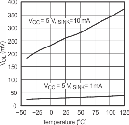
| IOL | SDA | VOL = 0.4 V | 4.5 V to 5.5 V |
3 | mA | |||
| P port | VOL = 0.4 V | 4.5 V to 5.5 V |
5 | 15 | ||||
| VOL = 1 V | 10 | 25 | ||||||
| INT | VOL = 0.4 V | 4.5 V to 5.5 V |
1.6 | |||||
| II | SCL, SDA | VI = VCC or GND | 4.5 V to 5.5 V |
±2 | μA | |||
| A0, A1, A2 | ±1 | |||||||
| IIHL | P port | VI ≥ VCC or VI ≤ GND | 4.5 V to 5.5 V |
±400 | μA | |||
| ICC | Operating mode | VI = VCC or GND, | IO = 0, fSCL = 400 kHz | 5.5 V | 100 | 200 | μA | |
| Standby mode | VI = VCC or GND, | IO = 0, fSCL = 0 kHz | 2.5 | 10 | ||||
| ΔICC | Supply current increase | One input at VCC – 0.6 V, Other inputs at VCC or GND |
4.5 V to 5.5 V |
200 | μA | |||
| Ci | SCL | VI = VCC or GND | 4.5 V to 5.5 V |
3 | 7 | pF | ||
| Cio | SDA | VIO = VCC or GND | 4.5 V to 5.5 V |
3 | 7 | pF | ||
| P port | 4 | 10 | ||||||
(1) All typical values are at VCC = 5 V, TA = 25°C.
(2) The power-on reset circuit resets the I2C bus logic with VCC < VPOR and sets all I/Os to logic high (with current source to VCC).
6.6 I2C Interface Timing Requirements
over recommended operating free-air temperature range (unless otherwise noted) (see Figure 7)| MIN | MAX | UNIT | |||
|---|---|---|---|---|---|
| fscl | I2C clock frequency | 400 | kHz | ||
| tsch | I2C clock high time | 0.6 | μs | ||
| tscl | I2C clock low time | 1.3 | μs | ||
| tsp | I2C spike time | 50 | ns | ||
| tsds | I2C serial-data setup time | 100 | ns | ||
| tsdh | I2C serial-data hold time | 0 | ns | ||
| ticr | I2C input rise time | 20 + 0.1Cb(1) | 300 | ns | |
| ticf | I2C input fall time | 20 + 0.1Cb(1) | 300 | ns | |
| tocf | I2C output fall time (10-pF to 400-pF bus) | 300 | ns | ||
| tbuf | I2C bus free time between stop and start | 1.3 | μs | ||
| tsts | I2C start or repeated start condition setup | 0.6 | μs | ||
| tsth | I2C start or repeated start condition hold | 0.6 | μs | ||
| tsps | I2C stop condition setup | 0.6 | μs | ||
| tvd | Valid-data time | SCL low to SDA output valid | 1.2 | μs | |
| Cb | I2C bus capacitive load | 400 | pF |
(1) Cb = total bus capacitance of one bus line in pF
6.7 Switching Characteristics
over recommended operating free-air temperature range, CL ≤ 100 pF (unless otherwise noted) (see Figure 8 and Figure 9)| PARAMETER | FROM (INPUT) |
TO (OUTPUT) |
MIN | MAX | UNIT | |
|---|---|---|---|---|---|---|
| tiv | Interrupt valid time | P port | INT | 4 | μs | |
| tir | Interrupt reset delay time | SCL | INT | 4 | μs | |
| tpv | Output data valid | SCL | P port | 4 | μs | |
| tsu | Input data setup time | P port | SCL | 0 | μs | |
| th | Input data hold time | P port | SCL | 4 | μs | |
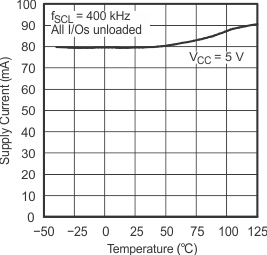
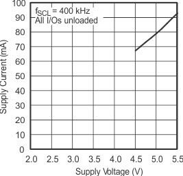
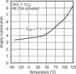
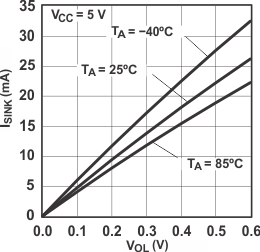
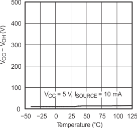
6.8 Typical Characteristics
TA = 25°C (unless otherwise noted)