SBVS032J March   2002  – July 2025 REF30 , REF30E

PRODUCTION DATA  

  1.   1
  2. Features
  3. Applications
  4. Description
  5. Device Comparison Table
  6. Pin Configuration and Functions
  7. Specifications
    1. 6.1 Absolute Maximum Ratings
    2. 6.2 ESD Ratings
    3. 6.3 Recommended Operating Conditions
    4. 6.4 Thermal Information
    5. 6.5 REF30E
    6. 6.6 REF30
    7. 6.7 Typical Characteristics REF30E
    8. 6.8 Typical Characteristics REF30
  8. Detailed Description
    1. 7.1 Overview
    2. 7.2 Functional Block Diagram
    3. 7.3 Feature Description
      1. 7.3.1 Supply Voltage
      2. 7.3.2 Thermal Hysteresis
      3. 7.3.3 Temperature Drift
      4. 7.3.4 Noise Performance
      5. 7.3.5 Long-Term Stability
      6. 7.3.6 Load Regulation
    4. 7.4 Device Functional Modes
      1. 7.4.1 Negative Reference Voltage
      2. 7.4.2 Data Acquisition
  9. Application and Implementation
    1. 8.1 Application Information
    2. 8.2 Typical Application
      1. 8.2.1 Design Requirements
      2. 8.2.2 Detailed Design Procedure
      3. 8.2.3 Application Curves
    3. 8.3 Power Supply Recommendations
    4. 8.4 Layout
      1. 8.4.1 Layout Guidelines
      2. 8.4.2 Layout Example
  10. Device and Documentation Support
    1. 9.1 Documentation Support
      1. 9.1.1 Related Documentation
    2. 9.2 Related Links
    3. 9.3 Receiving Notification of Documentation Updates
    4. 9.4 Support Resources
    5. 9.5 Trademarks
    6. 9.6 Electrostatic Discharge Caution
    7. 9.7 Glossary
  11. 10Revision History
  12. 11Mechanical, Packaging, and Orderable Information

Package Options

Mechanical Data (Package|Pins)
Thermal pad, mechanical data (Package|Pins)
Orderable Information

Typical Characteristics REF30

at TA = 25°C, VIN = 5V, and REF3025 used for typical characteristics (unless otherwise noted)

REF30 REF30E Temperature Drift
0°C to 70°C
Figure 6-8 Temperature Drift
REF30 REF30E Output Voltage vs Temperature
Figure 6-10 Output Voltage vs Temperature
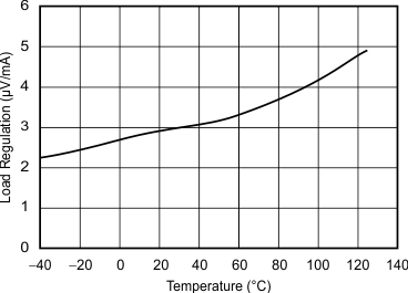
REF30 REF30E Load Regulation vs Temperature
Figure 6-12 Load Regulation vs Temperature
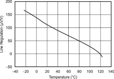
REF30 REF30E Line Regulation vs Temperature
Figure 6-14 Line Regulation vs Temperature
REF30 REF30E Power-Supply Rejection Ratio vs Frequency
Figure 6-16 Power-Supply Rejection Ratio vs Frequency
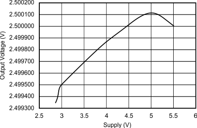
REF30 REF30E Output Voltage vs Supply Voltage
ILOAD = 25mA
Figure 6-18 Output Voltage vs Supply Voltage
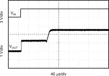
REF30 REF30E Step Response
CL = 0, 3V Startup
Figure 6-20 Step Response
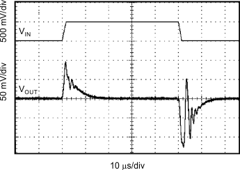
REF30 REF30E Line Transient Response
Figure 6-22 Line Transient Response
REF30 REF30E 0mA to 5mA Load
            Transient
CL = 0
Figure 6-24 0mA to 5mA Load Transient
REF30 REF30E 1mA to 25mA Load
            Transient
CL = 1μF
Figure 6-26 1mA to 25mA Load Transient
REF30 REF30E Long-Term Stability: 0 to 1000 Hours
Figure 6-28 Long-Term Stability: 0 to 1000 Hours
REF30 REF30E Long-Term Stability: 0 to 2000 Hours
Figure 6-30 Long-Term Stability: 0 to 2000 Hours
REF30 REF30E Temperature Drift
–40°C to +125°C
Figure 6-9 Temperature Drift
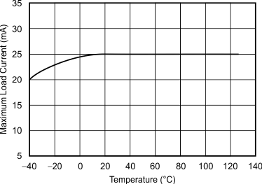
REF30 REF30E Maximum Load Current vs Temperature
Figure 6-11 Maximum Load Current vs Temperature
REF30 REF30E Quiescent Current vs Temperature
Figure 6-13 Quiescent Current vs Temperature
REF30 REF30E Output Impedance vs Frequency
Figure 6-15 Output Impedance vs Frequency
REF30 REF30E Output Voltage vs Supply Voltage
No Load
Figure 6-17 Output Voltage vs Supply Voltage
REF30 REF30E Output Voltage vs Load Current
Figure 6-19 Output Voltage vs Load Current
REF30 REF30E Step Response
CL = 0, 5V startup
Figure 6-21 Step Response
REF30 REF30E 0mA to 1mA Load
            Transient
CL = 0
Figure 6-23 0mA to 1mA Load Transient
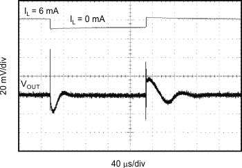
REF30 REF30E 1mA to 6mA Load
            Transient
CL = 1μF
Figure 6-25 1mA to 6mA Load Transient
REF30 REF30E 0.1Hz to 10Hz
            Noise
Figure 6-27 0.1Hz to 10Hz Noise
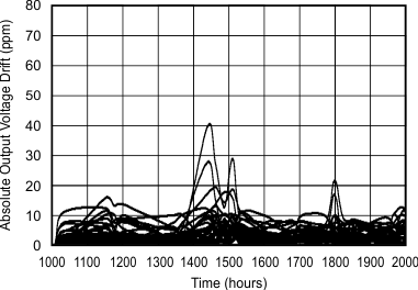
REF30 REF30E Long-Term Stability: 1000 to 2000 Hours
Figure 6-29 Long-Term Stability: 1000 to 2000 Hours