SLLS007E July 1985 – March 2024 SN75ALS192
PRODUCTION DATA
- 1
- 1 Features
- 2 Applications
- 3 Description
- 4 Pin Configuration and Functions
-
5 Specifications
- 5.1 Absolute Maximum Ratings
- 5.2 Dissipation Rating Table
- 5.3 Recommended Operating Conditions
- 5.4 Thermal Information
- 5.5 Electrical Characteristics
- 5.6 Switching Characteristics
- 5.7 Typical Characteristics Operation of the device at these or any other conditions beyond those indicated under “recommended operating conditions” is not implied.
- 6 Parameter Measurement Information
- 7 Device Functional Modes
- 8 Device and Documentation Support
- 9 Revision History
- 10Mechanical, Packaging, and Orderable Information
Package Options
Refer to the PDF data sheet for device specific package drawings
Mechanical Data (Package|Pins)
- NS|16
- N|16
- D|16
Thermal pad, mechanical data (Package|Pins)
Orderable Information
3 Description
The four differential line drivers are designed for data transmission over twisted-pair or parallel-wire transmission lines. They meet the requirements of ANSI Standard EIA/TIA-422-B and ITU Recommendations V.11 and are compatible with 3-state TTL circuits. Advanced low-power Schottky technology provides high speed without the usual power penalties. Standby supply current is typically only 26mA, while typical propagation delay time is less than 10ns.
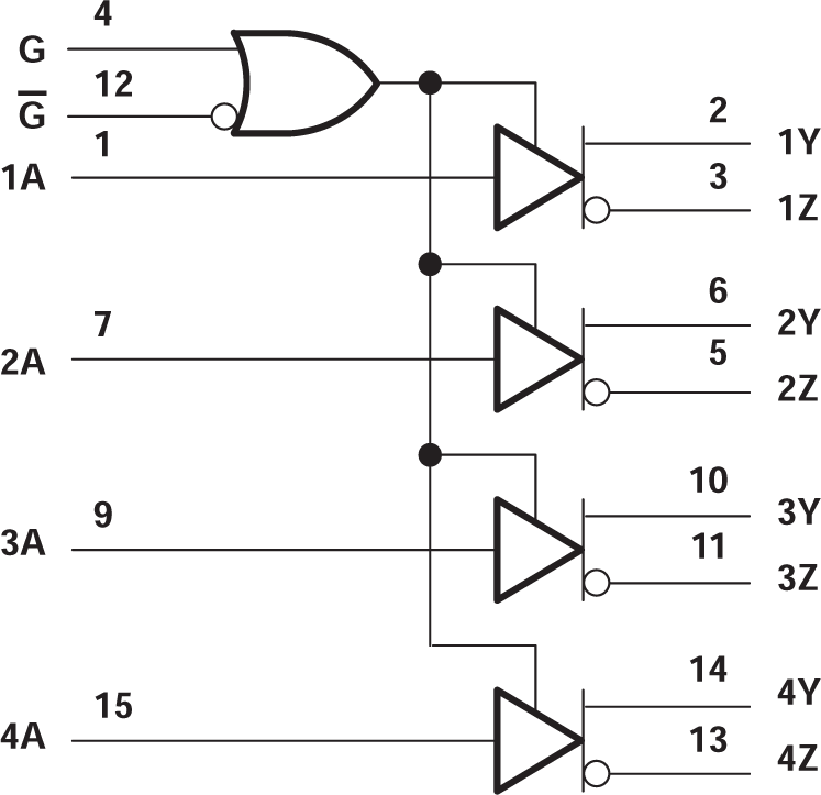
High-impedance inputs maintain low input currents, less than µA for a high level and less than 100µA for a low level. Complementary output-enable inputs (G and G) allow these devices to be enabled at either a high input level or low input level. The SN75ALS192 is capable of data rates in excess of 20 Mbit/s and is designed to operate with the SN75ALS193 quadruple line receiver.
The SN75ALS192 is characterized for operation from 0°C to 70°C.
| PART NUMBER | PACKAGE(1) | PACKAGE SIZE(2) |
|---|---|---|
| SN75ALS192 | SOIC (D, 16) | 9.9mm × 6mm |
| SO (NS, 16) | 10.2mm × 7.8mm |
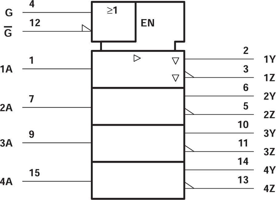
 Logic Symbol(1)
 Logic Diagram (Positive Logic)