SNLS698A April 2021 – September 2023 TDES960
PRODUCTION DATA
- 1
- 1 Features
- 2 Applications
- 3 Description
- 4 Revision History
- 5 Pin Configuration and Functions
-
6 Specifications
- 6.1 Absolute Maximum Ratings
- 6.2 ESD Ratings
- 6.3 Recommended Operating Conditions
- 6.4 Thermal Information
- 6.5 DC Electrical Characteristics
- 6.6 AC Electrical Characteristics
- 6.7 CSI-2 Timing Specifications
- 6.8 Recommended Timing for the Serial Control Bus
- 6.9 Timing Diagrams
- 6.10 Typical Characteristics
-
7 Detailed Description
- 7.1 Overview
- 7.2 Functional Block Diagram
- 7.3 Feature Description
- 7.4
Device Functional Modes
- 7.4.1 CSI-2 Mode
- 7.4.2 RAW Mode
- 7.4.3 MODE Pin
- 7.4.4 REFCLK
- 7.4.5 Receiver Port Control
- 7.4.6 Input Jitter Tolerance
- 7.4.7 Adaptive Equalizer
- 7.4.8 Channel Monitor Loop-Through Output Driver
- 7.4.9 RX Port Status
- 7.4.10 Sensor Status
- 7.4.11 GPIO Support
- 7.4.12 RAW Mode LV / FV Controls
- 7.4.13 CSI-2 Protocol Layer
- 7.4.14 CSI-2 Short Packet
- 7.4.15 CSI-2 Long Packet
- 7.4.16 CSI-2 Data Identifier
- 7.4.17 Virtual Channel and Context
- 7.4.18 CSI-2 Mode Virtual Channel Mapping
- 7.4.19 CSI-2 Transmitter Frequency
- 7.4.20 CSI-2 Output Bandwidth
- 7.4.21 CSI-2 Transmitter Status
- 7.4.22 Video Buffers
- 7.4.23 CSI-2 Line Count and Line Length
- 7.4.24 FrameSync Operation
- 7.4.25
CSI-2 Forwarding
- 7.4.25.1 Best-Effort Round Robin CSI-2 Forwarding
- 7.4.25.2 Synchronized CSI-2 Forwarding
- 7.4.25.3 Basic Synchronized CSI-2 Forwarding
- 7.4.25.4 Line-Interleaved CSI-2 Forwarding
- 7.4.25.5 Line-Concatenated CSI-2 Forwarding
- 7.4.25.6 CSI-2 Replicate Mode
- 7.4.25.7 CSI-2 Transmitter Output Control
- 7.4.25.8 Enabling and Disabling CSI-2 Transmitters
- 7.5
Programming
- 7.5.1 Serial Control Bus
- 7.5.2 Second I2C Port
- 7.5.3 I2C Target Operation
- 7.5.4 Remote Target Operation
- 7.5.5 Remote Target Addressing
- 7.5.6 Broadcast Write to Remote Devices
- 7.5.7 I2C Controller Proxy
- 7.5.8 I2C Controller Proxy Timing
- 7.5.9 Interrupt Support
- 7.5.10 Error Handling
- 7.5.11 Timestamp – Video Skew Detection
- 7.5.12 Pattern Generation
- 7.5.13 V3Link BIST Mode
- 7.6 Register Maps
- 8 Application and Implementation
- 9 Device and Documentation Support
- 10Mechanical, Packaging, and Orderable Information
Package Options
Mechanical Data (Package|Pins)
- RTD|64
Thermal pad, mechanical data (Package|Pins)
- RTD|64
Orderable Information
7.4.20 CSI-2 Output Bandwidth
During normal operation, CSI-2 transmitter output bandwidth is reduced as it needs to transition between Low-Power and High-Speed modes. The minimum CSI-2 High-Speed data transmission overhead consists of TLPX, THS-PREPARE, THS-ZERO, THS-SYNC, THS-TRAIL, and THS-EXIT as shown in Figure 6-6 . The bandwidth is further reduced when operating in Discontinuous CSI-2 Clock mode as the CSI-2 clock requires additional overhead time to transition between Low-Power and Clock Transmission modes. The minimum CSI-2 Discontinuous Clock timing overhead consists of TCLK-POST, TCLK-TRAIL, TCLK-PREPARE, TCLK-ZERO, and TCLK-PRE as shown in Figure 6-7 . The typical CSI-2 timing overhead is given in Table 7-15.
| CSI-2 TX Data Rate | CSI-2 TX Overhead, tCSI_Overhead [µs] | |
|---|---|---|
| Continuous CSI-2 Clock (0x33[1]=1) | Discontinuous CSI-2 Clock (0x33[1]=0) | |
| 1.664 Gbps | 0.73 | 1.68 |
| 1.6 Gbps | 0.76 | 1.74 |
| 1.472 Gbps | 0.83 | 1.89 |
| 1.2 Gbps | 0.91 | 1.92 |
| 800 Mbps | 0.93 | 2.06 |
| 400 Mbps | 1.30 | 2.65 |
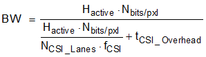
For Best-Effort Round Robin, Basic Synchronized or Line-Interleaved CSI-2 Forwarding, the maximum CSI-2 bandwidth for each CSI-2 port is defined in Equation 2.
For Line-Concatenated CSI-2 Forwarding, the maximum CSI-2 output bandwidth for each CSI-2 port is defined in Equation 3.
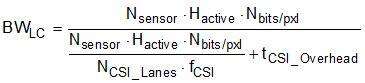
where
- Nsensor is the number of sensors attached to the TDES960
- Hactive is the horizontal line length of the active video frame in pixels
- Nbits/pxl is the number of bits per pixel
- NCSI_Lanes is the number of CSI-2 Lanes
- fCSI is the CSI-2 TX data rate per lane in Hz
- tCSI_Overhead is the CSI-2 High-speed data and clock timing overhead as given in Table 7-15
Equations (2) and (3) only apply when all aggregated sensors have identical video parameters, including pixels, lines, and frame rates. For aggregation BW calculation in mixed-sensor aggregation applications, contact TI for additional calculator tools.