SBOS932C January   2020  – March 2021 THP210

PRODUCTION DATA  

  1. Features
  2. Applications
  3. Description
  4. Revision History
  5. Pin Configuration and Functions
  6. Specifications
    1. 6.1 Absolute Maximum Ratings
    2. 6.2 ESD Ratings
    3. 6.3 Recommended Operating Conditions
    4. 6.4 Thermal Information
    5. 6.5 Electrical Characteristics
    6. 6.6 Typical Characteristics
  7. Parameter Measurement Information
    1. 7.1 Characterization Configuration
  8. Detailed Description
    1. 8.1 Overview
    2. 8.2 Functional Block Diagram
    3. 8.3 Feature Description
      1. 8.3.1 Super-Beta Input Bipolar Transistors
      2. 8.3.2 Power Down
      3. 8.3.3 Flexible Gain Setting
      4. 8.3.4 Amplifier Overload Power Limit
      5. 8.3.5 Unity Gain Stability
    4. 8.4 Device Functional Modes
  9. Application and Implementation
    1. 9.1 Application Information
      1. 9.1.1 I/O Headroom Considerations
      2. 9.1.2 DC Precision Analysis
        1. 9.1.2.1 DC Error Voltage at Room Temperature
        2. 9.1.2.2 DC Error Voltage Over Temperature
      3. 9.1.3 Noise Analysis
      4. 9.1.4 Mismatch of External Feedback Network
      5. 9.1.5 Operating the Power-Down Feature
      6. 9.1.6 Driving Capacitive Loads
      7. 9.1.7 Driving Differential ADCs
        1. 9.1.7.1 RC Filter Selection (Charge Kickback Filter)
        2. 9.1.7.2 Settling Time Driving the ADC Sample-and-Hold Operating Behavior
        3. 9.1.7.3 THD Performance
    2. 9.2 Typical Applications
      1. 9.2.1 MFB Filter
        1. 9.2.1.1 Design Requirements
        2. 9.2.1.2 Detailed Design Procedure
        3. 9.2.1.3 Application Curve
      2. 9.2.2 ADS891x With Single-Ended RC Filter Stage
        1. 9.2.2.1 Design Requirements
          1. 9.2.2.1.1 Measurement Results
      3. 9.2.3 Attenuation Configuration Drives the ADS8912B
        1. 9.2.3.1 Design Requirements
          1. 9.2.3.1.1 Measurement Results
  10. 10Power Supply Recommendations
  11. 11Layout
    1. 11.1 Layout Guidelines
      1. 11.1.1 Board Layout Recommendations
    2. 11.2 Layout Example
  12. 12Device and Documentation Support
    1. 12.1 Device Support
      1. 12.1.1 Development Support
    2. 12.2 Documentation Support
      1. 12.2.1 Related Documentation
    3. 12.3 Receiving Notification of Documentation Updates
    4. 12.4 Support Resources
    5. 12.5 Trademarks
    6. 12.6 Electrostatic Discharge Caution
    7. 12.7 Glossary
  13. 13Mechanical, Packaging, and Orderable Information

Package Options

Mechanical Data (Package|Pins)
Thermal pad, mechanical data (Package|Pins)
Orderable Information

Operating the Power-Down Feature

The power-down feature on the THP210 puts the device into a low power-consumption state, with quiescent current minimized. To force the device into the low-power state, drive the PD pin lower than the power-down threshold voltage (VVS+ – 2 V). Driving the PD pin lower than the power-down threshold voltage forces the internal logic to disable both the differential and common-mode amplifiers. The PD pin has an internal pullup current that allows the pin to be used in an open-drain MOSFET configuration without an additional pullup resistor, as seen in Figure 9-7. In this configuration, the logic level can be referenced to the MOSFET, and the voltage at the PD pin is level-shifted to account for use with high supply voltages. Be sure to select an N-type MOSFET with a maximum BVDSS greater than the total supply voltage.
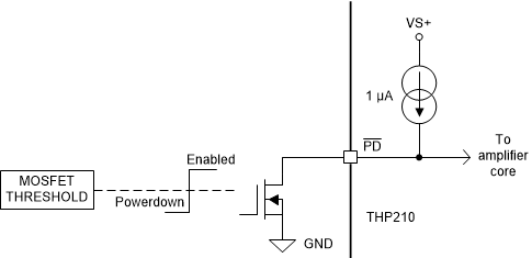
GUID-C299691B-8BFB-49D6-B2B7-C27AF816647A-low.gifFigure 9-7 Power-Down ( PD) Pin Interface With Low-Voltage Logic Level Signals

For applications that do not use the power-down feature, tie the PD pin to the positive supply voltage.

When PD is low (device is in power down) the output pins is in a high-impedance state.