SBOS874D August 2017 – February 2021 THS4561
PRODUCTION DATA
- 1 Features
- 2 Applications
- 3 Description
- 4 Revision History
- 5 Device Comparison Table
- 6 Pin Configuration and Functions
-
7 Specifications
- 7.1 Absolute Maximum Ratings
- 7.2 ESD Ratings
- 7.3 Recommended Operating Conditions
- 7.4 Thermal Information
- 7.5 Electrical Characteristics: VS+ – VS– = 5 V to 12 V
- 7.6 Typical Characteristics: (VS+) – (VS–) = 12 V
- 7.7 Typical Characteristics: (VS+) – (VS–) = 5 V
- 7.8 Typical Characteristics: (VS+) – (VS–) = 3 V
- 7.9 Typical Characteristics: (VS+) – (VS–) = 3-V to 12-V Supply Range
-
8 Parameter Measurement Information
- 8.1 Example Characterization Circuits
- 8.2 Output Interface Circuit for DC-Coupled Differential Testing
- 8.3 Output Common-Mode Measurements
- 8.4 Differential Amplifier Noise Measurements
- 8.5 Balanced Split-Supply Versus Single-Supply Characterization
- 8.6 Simulated Characterization Curves
- 8.7 Terminology and Application Assumptions
- 9 Detailed Description
- 10Application and Implementation
- 11Power Supply Recommendations
- 12Layout
- 13Device and Documentation Support
- 14Mechanical, Packaging, and Orderable Information
Package Options
Mechanical Data (Package|Pins)
Thermal pad, mechanical data (Package|Pins)
Orderable Information
10.2.3 Application Curves
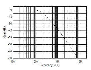
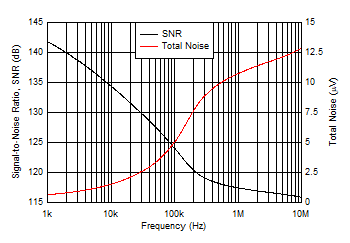
Figure 10-8 and Figure 10-9 show the gain response and the noise results of the circuit shown in Figure 10-7. Figure 10-7 shows a place for a differential input capacitor (shown as 100 fF) but is not used for the simulation results shown in this section. Results in Figure 10-8 illustrate a flat Butterworth filter response at the output nodes going to the ADC. Obtaining the SNR to the ADC input pins, and assuming an 8-VPP full scale (2.83 VRMS), gives the result of Figure 10-9. The 116-dB SNR and 13-µVRMS total noise shown in Figure 10-9 does not limit the performance for any SAR application.
 Figure 10-8 Gain Plot for a 170-kHz
Butterworth Filter
 Figure 10-9 Signal-to-Noise Ratio and
Total Noise Plot