SNVSBY3A November 2020 – April 2021 TLV840-Q1
PRODUCTION DATA
- 1 Features
- 2 Applications
- 3 Description
- 4 Revision History
- 5 Device Comparison
- 6 Pin Configuration and Functions
- 7 Specifications
- 8 Detailed Description
- 9 Application and Implementation
- 10Power Supply Recommendations
- 11Layout
- 12Device and Documentation Support
- 13Mechanical, Packaging, and Orderable Information
Package Options
Mechanical Data (Package|Pins)
- DBV|5
Thermal pad, mechanical data (Package|Pins)
Orderable Information
8.3.2 User-Programmable Reset Time Delay
The reset time delay can be set to a minimum value of 80 µs by leaving the CT pin floating, or a maximum value of approximately 6.2 seconds by connecting 10 µF delay capacitor. The reset time delay (tD) can be programmed by connecting a capacitor no larger than 10 µF between CT pin and GND.
The relationship between external capacitor (CCT) in µF at CT pin and the time delay (tD) in seconds is given by Equation 2.
Equation 3 solves for external capacitor (μF) by plugging RCT and tD (CT pin = Open) given in Section 7.5 section:
The reset delay varies according to three variables: the external capacitor (CCT), CT pin internal resistance (RCT) provided in Section 7.5, and a constant. The minimum and maximum variance due to the constant is show in Equation 4 and Equation 5:
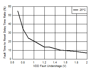
The recommended maximum delay capacitor for the TLV840-Q1 is limited to 10 µF as this ensures there is enough time for the capacitor to fully discharge when the reset condition occurs. When a voltage fault occurs, the previously charged up capacitor discharges, and if the monitored voltage returns from the fault condition before the delay capacitor discharges completely, the reset delay will be shorter than expected because the delay capacitor will begin charging from a voltage above zero. Larger delay capacitors can be used so long as the capacitor has enough time to fully discharge during the duration of the voltage fault. The amount of time required to discharge the delay capacitor relative to the reset delay increases as VDD overdrive increases as shown in Figure 8-3. From the graph below, to ensure the CT capacitor is fully discharged, the time period or duration of the voltage fault needs to be greater than 10% of the programmed reset time delay.
 Figure 8-3 CCT Discharge Time
During Fault Condition (VIT- = 2 V, CCT = 1 µF)