SNVSBY3A November 2020 – April 2021 TLV840-Q1
PRODUCTION DATA
- 1 Features
- 2 Applications
- 3 Description
- 4 Revision History
- 5 Device Comparison
- 6 Pin Configuration and Functions
- 7 Specifications
- 8 Detailed Description
- 9 Application and Implementation
- 10Power Supply Recommendations
- 11Layout
- 12Device and Documentation Support
- 13Mechanical, Packaging, and Orderable Information
Package Options
Mechanical Data (Package|Pins)
- DBV|5
Thermal pad, mechanical data (Package|Pins)
Orderable Information
8.3.3 Manual Reset (MR) Input
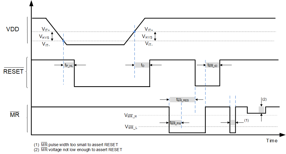
The manual reset (MR)
input allows a processor GPIO or other logic circuits to initiate a reset. A logic low on
MR with pulse duration longer than
tMR_PW will cause the reset output to assert. After
MR returns to a logic high
(VMR_H) and VDD is above VIT+, reset is
deasserted after the user programmed reset time delay (tD) expires.
The minimum duration for which MR is held under VMR_L must be at least 1% of tMR_tD. Otherwise, the effective reset delay will be shorter roughly by the difference between 1% of tMR_tD and the actual MR pulse width. For large capacitor based delays this difference could be noticeable unless care is taken to lengthen the MR pulse width.
MR is internally connected to VDD through a pull-up resistor RMR shown in Section 8.2. If the logic signal controlling MR is less than VDD, then additional current flows from VDD into MR internally. For minimum current consumption, drive MR to either VDD or GND. VMR should not be higher than VDD voltage.
 Figure 8-4 Timing Diagram MR
and RESET