SBOS966H april 2019 – june 2023 TLV9061-Q1 , TLV9062-Q1 , TLV9064-Q1
PRODMIX
- 1
- 1 Features
- 2 Applications
- 3 Description
- 4 Revision History
- 5 Description (continued)
- 6 Device Comparison Table
- 7 Pin Configuration and Functions
- 8 Specifications
- 9 Detailed Description
- 10Application and Implementation
- 11Device and Documentation Support
- 12Mechanical, Packaging, and Orderable Information
Package Options
Mechanical Data (Package|Pins)
Thermal pad, mechanical data (Package|Pins)
Orderable Information
3 Description
The TLV9061-Q1 (single), TLV9062-Q1 (dual) and TLV9064-Q1 (quad) are single-, dual- and quad-low-voltage (1.8 V to 5.5 V) operational amplifiers (op amps) with rail-to-rail input- and output-swing capabilities. These devices are cost-effective methods for automotive applications where low-voltage operation, a small footprint, and high capacitive load drive are required. Although the capacitive load drive of the TLV906x-Q1 is 100 pF, the resistive open-loop output impedance makes stabilizing with higher capacitive loads simpler. These op amps are designed specifically for low-voltage operation (1.8 V to 5.5 V) with performance specifications similar to the OPAx316 and TLVx316 devices, and identical to their non-automotive qualified TLV906x counterparts.
| PART NUMBER(2) | CHANNEL COUNT | PACKAGE(1) | PACKAGE SIZE(3) |
|---|---|---|---|
| TLV9061-Q1 | Single | DBV (SOT-23, 5) | 2.90 mm × 2.80 mm |
| DCK (SC70, 5) | 2.00 mm × 2.2 mm | ||
| TLV9061S-Q1 | Single with shutdown | DBV (SOT-23, 6) | 2.90 mm × 2.80 mm |
| TLV9062-Q1 | Dual | D (SOIC, 8) | 4.90 mm × 6.00 mm |
| PW (TSSOP, 8) | 3.00 mm × 6.40 mm | ||
| DGK (VSSOP, 8) | 3.00 mm × 4.90 mm | ||
| TLV9064-Q1 | Quad | D (SOIC, 14) | 8.65 mm × 6.00 mm |
| PW (TSSOP, 14) | 5.00 mm × 6.40 mm |
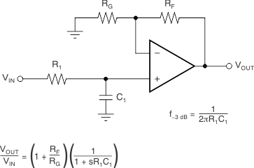
 Single-Pole, Low-Pass Filter