SNIS217C december 2020 – may 2023 TMP139
PRODUCTION DATA
- 1 Features
- 2 Applications
- 3 Description
- 4 Revision History
- 5 Pin Configuration and Functions
- 6 Specifications
-
7 Detailed Description
- 7.1 Overview
- 7.2 Functional Block Diagram
- 7.3 Feature Description
- 7.4 Device Functional Modes
- 7.5 Programming
- 7.6 Register Map
- 8 Application and Implementation
- 9 Device and Documentation Support
- 10Mechanical, Packaging, and Orderable Information
Package Options
Refer to the PDF data sheet for device specific package drawings
Mechanical Data (Package|Pins)
- YAH|6
Thermal pad, mechanical data (Package|Pins)
Orderable Information
7.4.4.4 Host I3C Read Operation with PEC
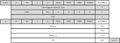
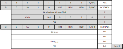
As shown in Figure 7-17 and Figure 7-18, when the PEC is enabled by the host, an additional byte is added by the host after sending the register address. The format for the additional byte is described in Table 7-5. Since only one and two byte reads are permitted by the CMD byte, the device shall terminate the read phase after sending one byte of data and PEC byte or two byte of data and PEC byte, followed by the T-bit as 0. In an unlikely case where the host sets the register address as 255, and attempts a read of two bytes, the device result is not guaranteed.
 Figure 7-17 I3C Basic Mode Read with PEC enabled
 Figure 7-18 I3C Basic Mode Read with PEC enabled and IBI Header
If the CMD value sent by the host is not valid for TMP139, the device shall NACK the read phase.
The TMP139 shall NACK the read phase of the transaction if there was a parity error in the write phase before the Repeated Start. If the host attempts to start a new transaction with a Repeated Start to the same device, then TMP139 shall NACK the device address to indicate an error condition to the host. The host must first clear the parity error condition before performing any new transfer to the TMP139.
If there is a PEC error, then the TMP139 shall NACK the read phase of the transaction. If the host attempts to start a new transaction with a Repeated Start to the same device, then TMP139 shall NACK the device address to indicate an existing error condition to the host. The host must first clear the PEC error condition before performing any new transfer to the TMP139.
When IBI is enabled, the device can communicate to the host the error conditions seen, using IBI. However when IBI is not enabled, it is strongly recommended that the host check the error status register to ensure that no parity or PEC error was detected on the bus.