SNIS217C december   2020  – may 2023 TMP139

PRODUCTION DATA  

  1. Features
  2. Applications
  3. Description
  4. Revision History
  5. Pin Configuration and Functions
  6. Specifications
    1. 6.1 Absolute Maximum Ratings
    2. 6.2 ESD Ratings
    3. 6.3 Recommended Operating Conditions
    4. 6.4 Thermal Information
    5. 6.5 Electrical Characteristics
    6. 6.6 Timing Requirements
    7. 6.7 Switching Characteristics
    8. 6.8 Timing Diagrams
    9. 6.9 Typical Characteristics
  7. Detailed Description
    1. 7.1 Overview
    2. 7.2 Functional Block Diagram
    3. 7.3 Feature Description
      1. 7.3.1 Power-Up Sequence
      2. 7.3.2 Power-Down and Device Reset
      3. 7.3.3 Temperature Result and Limits
      4. 7.3.4 Bus Reset
      5. 7.3.5 Interrupt Generation
      6. 7.3.6 Parity Error Check
      7. 7.3.7 Packet Error Check
    4. 7.4 Device Functional Modes
      1. 7.4.1 Conversion Mode
      2. 7.4.2 Serial Address
      3. 7.4.3 I2C Mode Operation
        1. 7.4.3.1 Host I2C Write Operation
        2. 7.4.3.2 Host I2C Read Operation
        3. 7.4.3.3 Host I2C Read Operation in Default Read Address Pointer Mode
        4. 7.4.3.4 Switching from I2C Mode to I3C Basic Mode
      4. 7.4.4 I3C Basic Mode Operation
        1. 7.4.4.1 Host I3C Write Operation without PEC
        2. 7.4.4.2 Host I3C Write Operation with PEC
        3. 7.4.4.3 Host I3C Read Operation without PEC
        4. 7.4.4.4 Host I3C Read Operation with PEC
        5. 7.4.4.5 Host I3C Read Operation in Default Read Address Pointer Mode
      5. 7.4.5 In Band Interrupt
        1. 7.4.5.1 In Band Interrupt Arbitration Rules
        2. 7.4.5.2 In Band Interrupt Bus Transaction
      6. 7.4.6 Common Command Codes Support
        1. 7.4.6.1 ENEC CCC
        2. 7.4.6.2 DISEC CCC
        3. 7.4.6.3 RSTDAA CCC
        4. 7.4.6.4 SETAASA CCC
        5. 7.4.6.5 GETSTATUS CCC
        6. 7.4.6.6 DEVCAP CCC
        7. 7.4.6.7 SETHID CCC
        8. 7.4.6.8 DEVCTRL CCC
      7. 7.4.7 I/O Operation
      8. 7.4.8 Timing Diagrams
    5. 7.5 Programming
      1. 7.5.1 Enabling Interrupt Mechanism
      2. 7.5.2 Clearing Interrupt
    6. 7.6 Register Map
  8. Application and Implementation
    1. 8.1 Application Information
    2. 8.2 Typical Application
      1. 8.2.1 Design Requirements
      2. 8.2.2 Detailed Design Procedure
      3. 8.2.3 Application Curves
    3. 8.3 Power Supply Recommendations
    4. 8.4 Layout
      1. 8.4.1 Layout Guidelines
      2. 8.4.2 Layout Example
  9. Device and Documentation Support
    1. 9.1 Receiving Notification of Documentation Updates
    2. 9.2 Support Resources
    3. 9.3 Trademarks
    4. 9.4 Electrostatic Discharge Caution
    5. 9.5 Glossary
  10. 10Mechanical, Packaging, and Orderable Information

Package Options

Refer to the PDF data sheet for device specific package drawings

Mechanical Data (Package|Pins)
  • YAH|6
Thermal pad, mechanical data (Package|Pins)
Orderable Information

Conversion Mode

The TMP139 powers up in continuous conversion mode. In this mode, the device shall perform temperature conversions every 125 ms as shown in Figure 7-5.
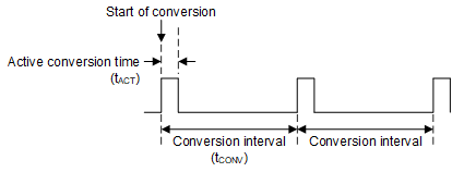
GUID-20201209-CA0I-XVP9-7ZLS-WK998FJGWQW2-low.gif Figure 7-5 Continuous Conversion Timing Diagram.
The application software can stop the conversion by clearing bit 0 of the MR26 register. When disabled, the device shall not update the result registers. When the temperature sensor is disabled, the host must wait for at least one active conversion cycle for the disable to take effect before any other writes are performed to the device. When the temperature sensor is re-enabled for continuous conversion mode, the host must wait for at least one conversion interval before reading the temperature results. During this time, read to other registers may be performed.