SPRS565D April   2009  – June 2014 TMS320C6743

PRODUCTION DATA.  

  1. 1TMS320C6743 Fixed- and Floating-Point Digital Signal Processor
    1. 1.1 Features
    2. 1.2 Applications
    3. 1.3 Description
    4. 1.4 Functional Block Diagram
  2. 2Revision History
  3. 3Device Overview
    1. 3.1 Device Characteristics
    2. 3.2 Device Compatibility
    3. 3.3 DSP Subsystem
      1. 3.3.1 C674x DSP CPU Description
      2. 3.3.2 DSP Memory Mapping
        1. 3.3.2.1 External Memories
        2. 3.3.2.2 DSP Internal Memories
        3. 3.3.2.3 C674x CPU
    4. 3.4 Memory Map Summary
      1. 3.4.1 C6743 Top Level Memory Map
    5. 3.5 Pin Assignments
      1. 3.5.1 Pin Map (Bottom View)
    6. 3.6 Terminal Functions
      1. 3.6.1  Device Reset and JTAG
      2. 3.6.2  High-Frequency Oscillator and PLL
      3. 3.6.3  External Memory Interface A (ASYNC)
      4. 3.6.4  External Memory Interface B (SDRAM only)
      5. 3.6.5  Serial Peripheral Interface Modules (SPI0)
      6. 3.6.6  Enhanced Capture/Auxiliary PWM Modules (eCAP0, eCAP1, eCAP2)
      7. 3.6.7  Enhanced Pulse Width Modulators (eHRPWM0, eHRPWM1, eHRPWM2)
      8. 3.6.8  Enhanced Quadrature Encoder Pulse Module (eQEP)
      9. 3.6.9  Boot
      10. 3.6.10 Universal Asynchronous Receiver/Transmitters (UART0, UART2)
      11. 3.6.11 Inter-Integrated Circuit Modules (I2C0, I2C1)
      12. 3.6.12 Timers
      13. 3.6.13 Multichannel Audio Serial Ports (McASP0, McASP1)
      14. 3.6.14 Ethernet Media Access Controller (EMAC)
      15. 3.6.15 Multimedia Card/Secure Digital (MMC/SD)
      16. 3.6.16 General-Purpose IO Only Terminal Functions
      17. 3.6.17 Reserved and No Connect Terminal Functions
      18. 3.6.18 Supply and Ground Terminal Functions
  4. 4Device Configuration
    1. 4.1 Boot Modes
    2. 4.2 SYSCFG Module
    3. 4.3 Pullup/Pulldown Resistors
  5. 5Device Operating Conditions
    1. 5.1 Absolute Maximum Ratings Over Operating Junction Temperature Range (Unless Otherwise Noted)
    2. 5.2 Handling Ratings
    3. 5.3 Recommended Operating Conditions
    4. 5.4 Notes on Recommended Power-On Hours (POH)
    5. 5.5 Electrical Characteristics Over Recommended Ranges of Supply Voltage and Operating Junction Temperature (Unless Otherwise Noted)
  6. 6Peripheral Information and Electrical Specifications
    1. 6.1  Parameter Information
      1. 6.1.1 Parameter Information Device-Specific Information
        1. 6.1.1.1 Signal Transition Levels
    2. 6.2  Recommended Clock and Control Signal Transition Behavior
    3. 6.3  Power Supplies
      1. 6.3.1 Power-On Sequence
      2. 6.3.2 Power-Off Sequence
    4. 6.4  Reset
      1. 6.4.1 Power-On Reset (POR)
      2. 6.4.2 Warm Reset
      3. 6.4.3 Reset Electrical Data Timings
    5. 6.5  Crystal Oscillator or External Clock Input
    6. 6.6  Clock PLLs
      1. 6.6.1 PLL Device-Specific Information
      2. 6.6.2 Device Clock Generation
      3. 6.6.3 PLL Controller 0 Registers
    7. 6.7  DSP Interrupts
    8. 6.8  General-Purpose Input/Output (GPIO)
      1. 6.8.1 GPIO Register Description(s)
      2. 6.8.2 GPIO Peripheral Input/Output Electrical Data/Timing
        1. Table 6-10 Timing Requirements for GPIO Inputs (see )
        2. Table 6-11 Switching Characteristics Over Recommended Operating Conditions for GPIO Outputs (see )
      3. 6.8.3 GPIO Peripheral External Interrupts Electrical Data/Timing
        1. Table 6-12 Timing Requirements for External Interrupts (see )
    9. 6.9  EDMA
    10. 6.10 External Memory Interface A (EMIFA)
      1. 6.10.1 EMIFA Asynchronous Memory Support
      2. 6.10.2 EMIFA Connection Examples
      3. 6.10.3 External Memory Interface (EMIF) Registers
      4. 6.10.4 EMIFA Electrical Data/Timing
        1. Table 6-19 EMIFA Asynchronous Memory Timing Requirements
        2. Table 6-20 EMIFA Asynchronous Memory Switching Characteristics
    11. 6.11 External Memory Interface B (EMIFB)
      1. 6.11.1 EMIFB SDRAM Loading Limitations
      2. 6.11.2 Interfacing to SDRAM
      3. 6.11.3 EMIFB Electrical Data/Timing
        1. Table 6-24 EMIFB SDRAM Interface Timing Requirements
        2. Table 6-25 EMIFB SDRAM Interface Switching Characteristics
    12. 6.12 Memory Protection Units
    13. 6.13 MMC / SD / SDIO (MMCSD)
      1. 6.13.1 MMCSD Peripheral Register Description(s)
      2. 6.13.2 MMC/SD Electrical Data/Timing
        1. Table 6-29 Timing Requirements for MMC/SD Module (see and )
        2. Table 6-30 Switching Characteristics Over Recommended Operating Conditions for MMC/SD Module (see through )
    14. 6.14 Ethernet Media Access Controller (EMAC)
      1. 6.14.1 EMAC Peripheral Register Description(s)
      2. 6.14.2 EMAC Electrical Data/Timing
    15. 6.15 Management Data Input/Output (MDIO)
      1. 6.15.1 MDIO Peripheral Register Description(s)
      2. 6.15.2 Management Data Input/Output (MDIO) Electrical Data/Timing
        1. Table 6-38 Timing Requirements for MDIO Input (see and )
        2. Table 6-39 Switching Characteristics Over Recommended Operating Conditions for MDIO Output (see )
    16. 6.16 Multichannel Audio Serial Ports (McASP0, McASP1)
      1. 6.16.1 McASP Peripheral Registers Description(s)
      2. 6.16.2 McASP Electrical Data/Timing
        1. 6.16.2.1 Multichannel Audio Serial Port 0 (McASP0) Timing
          1. Table 6-44 McASP0 Timing Requirements
          2. Table 6-45 McASP0 Switching Characteristics
        2. 6.16.2.2 Multichannel Audio Serial Port 1 (McASP1) Timing
          1. Table 6-46 McASP1 Timing Requirements
          2. Table 6-47 McASP1 Switching Characteristics
    17. 6.17 Serial Peripheral Interface Ports (SPI0)
      1. 6.17.1 SPI Peripheral Registers Description(s)
      2. 6.17.2 SPI Electrical Data/Timing
        1. 6.17.2.1 Serial Peripheral Interface (SPI) Timing
          1. Table 6-49 General Timing Requirements for SPI0 Master Modes
          2. Table 6-50 General Timing Requirements for SPI0 Slave Modes
          3. Table 6-51 Additional SPI0 Master Timings, 4-Pin Enable Option
          4. Table 6-52 Additional SPI0 Master Timings, 4-Pin Chip Select Option
          5. Table 6-53 Additional SPI0 Master Timings, 5-Pin Option
          6. Table 6-54 Additional SPI0 Slave Timings, 4-Pin Enable Option
          7. Table 6-55 Additional SPI0 Slave Timings, 4-Pin Chip Select Option
          8. Table 6-56 Additional SPI0 Slave Timings, 5-Pin Option
    18. 6.18 Enhanced Capture (eCAP) Peripheral
      1. Table 6-58 Enhanced Capture (eCAP) Timing Requirement
      2. Table 6-59 eCAP Switching Characteristics
    19. 6.19 Enhanced Quadrature Encoder (eQEP) Peripheral
      1. Table 6-61 Enhanced Quadrature Encoder Pulse (eQEP) Timing Requirements
      2. Table 6-62 eQEP Switching Characteristics
    20. 6.20 Enhanced Pulse Width Modulator (eHRPWM) Modules
      1. 6.20.1 Enhanced Pulse Width Modulator (eHRPWM) Timing
        1. Table 6-64 eHRPWM Timing Requirements
        2. Table 6-65 eHRPWM Switching Characteristics
      2. 6.20.2 Trip-Zone Input Timing
    21. 6.21 Timers
      1. 6.21.1 Timer Electrical Data/Timing
        1. Table 6-69 Timing Requirements for Timer Input (see )
        2. Table 6-70 Switching Characteristics Over Recommended Operating Conditions for Timer Output
    22. 6.22 Inter-Integrated Circuit Serial Ports (I2C0, I2C1)
      1. 6.22.1 I2C Device-Specific Information
      2. 6.22.2 I2C Peripheral Registers Description(s)
      3. 6.22.3 I2C Electrical Data/Timing
        1. 6.22.3.1 Inter-Integrated Circuit (I2C) Timing
          1. Table 6-72 I2C Input Timing Requirements
          2. Table 6-73 I2C Switching Characteristics
    23. 6.23 Universal Asynchronous Receiver/Transmitter (UART)
      1. 6.23.1 UART Peripheral Registers Description(s)
      2. 6.23.2 UART Electrical Data/Timing
        1. Table 6-75 Timing Requirements for UARTx Receive (see )
        2. Table 6-76 Switching Characteristics Over Recommended Operating Conditions for UARTx Transmit (see )
    24. 6.24 Power and Sleep Controller (PSC)
      1. 6.24.1 PSC Peripheral Registers Description(s)
      2. 6.24.2 Power Domain and Module Topology
        1. 6.24.2.1 Power Domain States
        2. 6.24.2.2 Module States
    25. 6.25 Programmable Real-Time Unit Subsystem (PRUSS)
      1. 6.25.1 PRUSS Register Descriptions
    26. 6.26 Emulation Logic
      1. 6.26.1 JTAG Port Description
      2. 6.26.2 Scan Chain Configuration Parameters
      3. 6.26.3 JTAG 1149.1 Boundary Scan Considerations
    27. 6.27 IEEE 1149.1 JTAG
      1. 6.27.1 JTAG Peripheral Register Description(s) – JTAG ID Register
      2. 6.27.2 JTAG Test-Port Electrical Data/Timing
        1. Table 6-91 Timing Requirements for JTAG Test Port (see )
        2. Table 6-92 Switching Characteristics Over Recommended Operating Conditions for JTAG Test Port (see )
  7. 7Device and Documentation Support
    1. 7.1 Device Support
      1. 7.1.1 Development Support
      2. 7.1.2 Device and Development-Support Tool Nomenclature
    2. 7.2 Documentation Support
    3. 7.3 Support Resources
    4. 7.4 Trademarks
    5. 7.5 Electrostatic Discharge Caution
    6. 7.6 Glossary
  8. 8Mechanical Packaging and Orderable Information
    1. 8.1 Thermal Data for ZKB
    2. 8.2 Thermal Data for PTP
    3. 8.3 Supplementary Information About the 176-pin PTP PowerPAD™ Package
      1. 8.3.1 Standoff Height
      2. 8.3.2 PowerPAD™ PCB Footprint
    4. 8.4 Mechanical Drawings

Package Options

Refer to the PDF data sheet for device specific package drawings

Mechanical Data (Package|Pins)
  • ZKB|256
  • PTP|176
Thermal pad, mechanical data (Package|Pins)
Orderable Information

Crystal Oscillator or External Clock Input

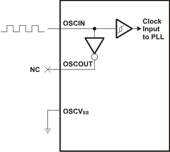
The device includes two choices to provide an external clock input, which is fed to the on-chip PLL to generate high-frequency system clocks. These options are illustrated in Figure 6-6 and Figure 6-7. For input clock frequencies between 12 and 20 MHz, a crystal with 80 ohm max ESR is recommended. For input clock frequencies between 20 and 30 MHz, a crystal with 60 ohm max ESR is recommended. Typical load capacitance values are 10-20 pF, where the load capacitance is the series combination of C1 and C2.

The CLKMODE bit in the PLLCTL register must be 0 to use the on-chip oscillator. If CLKMODE is set to 1, the internal oscillator is disabled.

  • Figure 6-6 illustrates the option that uses on-chip 1.2V oscillator with external crystal circuit.
  • Figure 6-7 illustrates the option that uses an external 1.2V clock input.
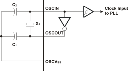
TMS320C6743 onchip_1-2v_osc_prs483.gifFigure 6-6 On-Chip 1.2V Oscillator

Table 6-2 Oscillator Timing Requirements

NO PARAMETER MIN MAX UNIT
fosc Oscillator frequency range (OSCIN/OSCOUT) 12 30 MHz
TMS320C6743 extended_1-2v_clock_prs483.gifFigure 6-7 External 1.2V Clock Source

Table 6-3 OSCIN Timing Requirements for Externally Driven Clock

NO MIN MAX UNIT
fOSCIN OSCIN frequency range (OSCIN) 12 50 MHz
tc(OSCIN) Cycle time, external clock driven on OSCIN 20 ns
tw(OSCINH) Pulse width high, external clock on OSCIN 0.4 tc(OSCIN) ns
tw(OSCINL) Pulse width low, external clock on OSCIN 0.4 tc(OSCIN) ns
tt(OSCIN) Transition time, OSCIN 0.25P or 10(1) ns
tj(OSCIN) Period jitter, OSCIN 0.02P ns
Whichever is smaller. P = the period of the applied signal. Maintaining transition times as fast as possible is recommended to improve noise immunity on input signals.