SPRS565D April 2009 – June 2014 TMS320C6743
PRODUCTION DATA.
- 1TMS320C6743 Fixed- and Floating-Point Digital Signal Processor
- 2Revision History
-
3Device Overview
- 3.1 Device Characteristics
- 3.2 Device Compatibility
- 3.3 DSP Subsystem
- 3.4 Memory Map Summary
- 3.5 Pin Assignments
- 3.6
Terminal Functions
- 3.6.1 Device Reset and JTAG
- 3.6.2 High-Frequency Oscillator and PLL
- 3.6.3 External Memory Interface A (ASYNC)
- 3.6.4 External Memory Interface B (SDRAM only)
- 3.6.5 Serial Peripheral Interface Modules (SPI0)
- 3.6.6 Enhanced Capture/Auxiliary PWM Modules (eCAP0, eCAP1, eCAP2)
- 3.6.7 Enhanced Pulse Width Modulators (eHRPWM0, eHRPWM1, eHRPWM2)
- 3.6.8 Enhanced Quadrature Encoder Pulse Module (eQEP)
- 3.6.9 Boot
- 3.6.10 Universal Asynchronous Receiver/Transmitters (UART0, UART2)
- 3.6.11 Inter-Integrated Circuit Modules (I2C0, I2C1)
- 3.6.12 Timers
- 3.6.13 Multichannel Audio Serial Ports (McASP0, McASP1)
- 3.6.14 Ethernet Media Access Controller (EMAC)
- 3.6.15 Multimedia Card/Secure Digital (MMC/SD)
- 3.6.16 General-Purpose IO Only Terminal Functions
- 3.6.17 Reserved and No Connect Terminal Functions
- 3.6.18 Supply and Ground Terminal Functions
- 4Device Configuration
-
5Device Operating Conditions
- 5.1 Absolute Maximum Ratings Over Operating Junction Temperature Range (Unless Otherwise Noted)
- 5.2 Handling Ratings
- 5.3 Recommended Operating Conditions
- 5.4 Notes on Recommended Power-On Hours (POH)
- 5.5 Electrical Characteristics Over Recommended Ranges of Supply Voltage and Operating Junction Temperature (Unless Otherwise Noted)
-
6Peripheral Information and Electrical Specifications
- 6.1 Parameter Information
- 6.2 Recommended Clock and Control Signal Transition Behavior
- 6.3 Power Supplies
- 6.4 Reset
- 6.5 Crystal Oscillator or External Clock Input
- 6.6 Clock PLLs
- 6.7 DSP Interrupts
- 6.8 General-Purpose Input/Output (GPIO)
- 6.9 EDMA
- 6.10 External Memory Interface A (EMIFA)
- 6.11 External Memory Interface B (EMIFB)
- 6.12 Memory Protection Units
- 6.13 MMC / SD / SDIO (MMCSD)
- 6.14 Ethernet Media Access Controller (EMAC)
- 6.15 Management Data Input/Output (MDIO)
- 6.16 Multichannel Audio Serial Ports (McASP0, McASP1)
- 6.17
Serial Peripheral Interface Ports (SPI0)
- 6.17.1 SPI Peripheral Registers Description(s)
- 6.17.2
SPI Electrical Data/Timing
- 6.17.2.1
Serial Peripheral Interface (SPI) Timing
- Table 6-49 General Timing Requirements for SPI0 Master Modes
- Table 6-50 General Timing Requirements for SPI0 Slave Modes
- Table 6-51 Additional SPI0 Master Timings, 4-Pin Enable Option
- Table 6-52 Additional SPI0 Master Timings, 4-Pin Chip Select Option
- Table 6-53 Additional SPI0 Master Timings, 5-Pin Option
- Table 6-54 Additional SPI0 Slave Timings, 4-Pin Enable Option
- Table 6-55 Additional SPI0 Slave Timings, 4-Pin Chip Select Option
- Table 6-56 Additional SPI0 Slave Timings, 5-Pin Option
- 6.17.2.1
Serial Peripheral Interface (SPI) Timing
- 6.18 Enhanced Capture (eCAP) Peripheral
- 6.19 Enhanced Quadrature Encoder (eQEP) Peripheral
- 6.20 Enhanced Pulse Width Modulator (eHRPWM) Modules
- 6.21 Timers
- 6.22 Inter-Integrated Circuit Serial Ports (I2C0, I2C1)
- 6.23 Universal Asynchronous Receiver/Transmitter (UART)
- 6.24 Power and Sleep Controller (PSC)
- 6.25 Programmable Real-Time Unit Subsystem (PRUSS)
- 6.26 Emulation Logic
- 6.27 IEEE 1149.1 JTAG
- 7Device and Documentation Support
- 8Mechanical Packaging and Orderable Information
Package Options
Refer to the PDF data sheet for device specific package drawings
Mechanical Data (Package|Pins)
- ZKB|256
- PTP|176
Thermal pad, mechanical data (Package|Pins)
- PTP|176
Orderable Information
6.18 Enhanced Capture (eCAP) Peripheral
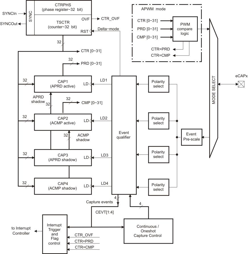
The device contains up to three enhanced capture (eCAP) modules. Figure 6-37 shows a functional block diagram of a module. See the TMS320C674x/OMAP-L1x Processor Peripherals Overview Reference Guide (SPRUFK9) for more details.
Uses for ECAP include:
- Speed measurements of rotating machinery (e.g. toothed sprockets sensed via Hall sensors)
- Elapsed time measurements between position sensor triggers
- Period and duty cycle measurements of Pulse train signals
- Decoding current or voltage amplitude derived from cuty cycle encoded current/voltage sensors
The ECAP module described in this specification includes the following features:
- 32 bit time base
- 4 event time-stamp registers (each 32 bits)
- Edge polarity selection for up to 4 sequenced time-stamp capture events
- Interrupt on either of the 4 events
- Single shot capture of up to 4 event time-stamps
- Continuous mode capture of time-stamps in a 4 deep circular buffer
- Absolute time-stamp capture
- Difference mode time-stamp capture
- All the above resources are dedicated to a single input pin
The eCAP modules are clocked at the SYSCLK2 rate.
 Figure 6-37 eCAP Functional Block Diagram
 Table 6-57 is the list of the ECAP registers.
Table 6-57 ECAPx Configuration Registers
| ECAP0
BYTE ADDRESS |
ECAP1
BYTE ADDRESS |
ECAP2
BYTE ADDRESS |
REGISTER NAME | REGISTER DESCRIPTION |
|---|---|---|---|---|
| 0x01F0 6000 | 0x01F0 7000 | 0x01F0 8000 | TSCTR | Time-Stamp Counter |
| 0x01F0 6004 | 0x01F0 7004 | 0x01F0 8004 | CTRPHS | Counter Phase Offset Value Register |
| 0x01F0 6008 | 0x01F0 7008 | 0x01F0 8008 | CAP1 | Capture 1 Register |
| 0x01F0 600C | 0x01F0 700C | 0x01F0 800C | CAP2 | Capture 2 Register |
| 0x01F0 6010 | 0x01F0 7010 | 0x01F0 8010 | CAP3 | Capture 3 Register |
| 0x01F0 6014 | 0x01F0 7014 | 0x01F0 8014 | CAP4 | Capture 4 Register |
| 0x01F0 6028 | 0x01F0 7028 | 0x01F0 8028 | ECCTL1 | Capture Control Register 1 |
| 0x01F0 602A | 0x01F0 702A | 0x01F0 802A | ECCTL2 | Capture Control Register 2 |
| 0x01F0 602C | 0x01F0 702C | 0x01F0 802C | ECEINT | Capture Interrupt Enable Register |
| 0x01F0 602E | 0x01F0 702E | 0x01F0 802E | ECFLG | Capture Interrupt Flag Register |
| 0x01F0 6030 | 0x01F0 7030 | 0x01F0 8030 | ECCLR | Capture Interrupt Clear Register |
| 0x01F0 6032 | 0x01F0 7032 | 0x01F0 8032 | ECFRC | Capture Interrupt Force Register |
| 0x01F0 605C | 0x01F0 705C | 0x01F0 805C | REVID | Revision ID |
Table 6-58 shows the eCAP timing requirement and Table 6-59 shows the eCAP switching characteristics.