SCDS408C February 2019 – December 2023 TMUX1111 , TMUX1112 , TMUX1113
PRODUCTION DATA
- 1
- 1 Features
- 2 Applications
- 3 Description
- 4 Device Comparison Table
- 5 Pin Configuration and Functions
-
6 Specifications
- 6.1 Absolute Maximum Ratings
- 6.2 ESD Ratings
- 6.3 Recommended Operating Conditions
- 6.4 Thermal Information
- 6.5 Electrical Characteristics (VDD = 5V ±10 %)
- 6.6 Electrical Characteristics (VDD = 3.3V ±10 %)
- 6.7 Electrical Characteristics (VDD = 1.8V ±10 %)
- 6.8 Electrical Characteristics (VDD = 1.2V ±10 %)
- 6.9 Typical Characteristics
- 7 Parameter Measurement Information
- 8 Detailed Description
- 9 Application and Implementation
- 10Device and Documentation Support
- 11Revision History
- 12Mechanical, Packaging, and Orderable Information
Package Options
Refer to the PDF data sheet for device specific package drawings
Mechanical Data (Package|Pins)
- PW|16
- RSV|16
Thermal pad, mechanical data (Package|Pins)
- RSV|16
Orderable Information
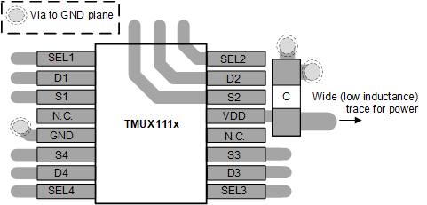
9.5.2 Layout Example
Figure 9-8 shows an example of a PCB layout with the TMUX111x. Some key considerations are:
- Decouple the VDD pin with a 0.1µF capacitor, placed as close to the pin as possible. Make sure that the capacitor voltage rating is sufficient for the VDD supply.
- Keep the input lines as short as possible.
- Use a solid ground plane to help reduce electromagnetic interference (EMI) noise pickup.
- Do not run sensitive analog traces in parallel with digital traces. Avoid crossing digital and analog traces if possible, and only make perpendicular crossings when necessary.
 Figure 9-8 TMUX111x
Layout Example