SCDS404B March 2021 – November 2022 TMUX7411F , TMUX7412F , TMUX7413F
PRODMIX
- 1 Features
- 2 Applications
- 3 Description
- 4 Revision History
- 5 Device Comparison Table
- 6 Pin Configuration and Functions
-
7 Specifications
- 7.1 Absolute Maximum Ratings
- 7.2 ESD Ratings
- 7.3 Thermal Information
- 7.4 Recommended Operating Conditions
- 7.5 Electrical Characteristics: Global
- 7.6 ±15 V Dual Supply: Electrical Characteristics
- 7.7 ±20 V Dual Supply: Electrical Characteristics
- 7.8 12 V Single Supply: Electrical Characteristics
- 7.9 36 V Single Supply: Electrical Characteristics
- 7.10 Typical Characteristics
-
8 Parameter Measurement Information
- 8.1 On-Resistance
- 8.2 Turn-On and Turn-Off Time
- 8.3 Off-Leakage Current
- 8.4 On-Leakage Current
- 8.5 Input and Output Leakage Current Under Overvoltage Fault
- 8.6 Fault Response Time
- 8.7 Fault Recovery Time
- 8.8 Fault Flag Response Time
- 8.9 Fault Flag Recovery Time
- 8.10 Charge Injection
- 8.11 Off Isolation
- 8.12 Inter-Channel Crosstalk
- 8.13 Bandwidth
- 8.14 THD + Noise
- 9 Detailed Description
- 10Application and Implementation
- 11Power Supply Recommendations
- 12Layout
- 13Device and Documentation Support
- 14Mechanical, Packaging, and Orderable Information
Package Options
Mechanical Data (Package|Pins)
- RRP|16
Thermal pad, mechanical data (Package|Pins)
Orderable Information
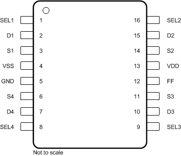
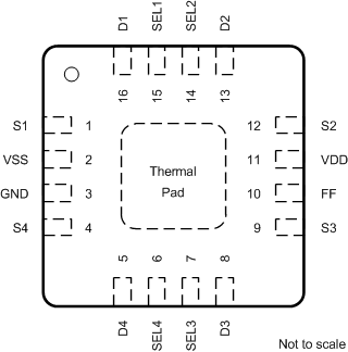
6 Pin Configuration and Functions
 Figure 6-1 (Preview) PW Package,
16-Pin TSSOP(Top View)
 Figure 6-2 RRP Package,
16-Pin WQFN(Top View)
Table 6-1 Pin Functions
| PIN | TYPE(1) | DESCRIPTION | ||
|---|---|---|---|---|
| NAME | TSSOP(2) | WQFN | ||
| D1 | 2 | 16 | I/O | Drain pin 1. Can be an input or output. The drain pin is not overvoltage protected. |
| D2 | 15 | 13 | I/O | Drain pin 2. Can be an input or output. The drain pin is not overvoltage protected. |
| D3 | 10 | 8 | I/O | Drain pin 3. Can be an input or output. The drain pin is not overvoltage protected. |
| D4 | 7 | 5 | I/O | Drain pin 4. Can be an input or output. The drain pin is not overvoltage protected. |
| FF | 12 | 10 | O | General fault flag. This pin is an open drain output and is asserted low when overvoltage condition is detected on any of the source (Sx) input pins. Connect this pin to an external supply (1.8 V to 5.5 V) through a 1 kΩ pull-up resistor. |
| GND | 5 | 3 | P | Ground (0 V) reference |
| S1 | 3 | 1 | I/O | Overvoltage protected source pin 1. Can be an input or output. |
| S2 | 14 | 12 | I/O | Overvoltage protected source pin 2. Can be an input or output. |
| S3 | 11 | 9 | I/O | Overvoltage protected source pin 3. Can be an input or output. |
| S4 | 6 | 4 | I/O | Overvoltage protected source pin 4. Can be an input or output. |
| SEL1 | 1 | 15 | I | Logic control input 1. |
| SEL2 | 16 | 14 | I | Logic control input 2. |
| SEL3 | 9 | 7 | I | Logic control input 3. |
| SEL4 | 8 | 6 | I | Logic control input 4. |
| VDD | 13 | 11 | P | Positive power supply. This pin is the most positive power-supply potential. Connect a decoupling capacitor ranging from 0.1 µF to 10 µF between VDD and GND for reliable operation. |
| VSS | 4 | 2 | P | Negative power supply. This pin is the most negative power-supply potential. This pin can be connected to ground in single-supply applications. Connect a decoupling capacitor ranging from 0.1 µF to 10 µF between VSS and GND for reliable operation. |
| Thermal Pad | — | The thermal pad is not connected internally. It is recommended that the pad be tied to GND or VSS for best performance. | ||
(1) I = input, O = output, I/O = input and output, P = power.
(2) Preview package.