SLASEN3B January 2018 – August 2018 TPA3220
PRODUCTION DATA.
- 1 Features
- 2 Applications
- 3 Description
- 4 Revision History
- 5 Device Comparison Table
- 6 Pin Configuration and Functions
-
7 Specifications
- 7.1 Absolute Maximum Ratings
- 7.2 ESD Ratings
- 7.3 Recommended Operating Conditions
- 7.4 Thermal Information
- 7.5 Electrical Characteristics
- 7.6 Audio Characteristics (BTL)
- 7.7 Audio Characteristics (PBTL)
- 7.8 Typical Characteristics, BTL Configuration, AD-mode
- 7.9 Typical Characteristics, PBTL Configuration, AD-mode
- 8 Parameter Measurement Information
-
9 Detailed Description
- 9.1 Overview
- 9.2 Functional Block Diagrams
- 9.3 Feature Description
- 9.4
Device Functional Modes
- 9.4.1 Powering Up
- 9.4.2 Powering Down
- 9.4.3 Device Reset
- 9.4.4 Device Soft Mute
- 9.4.5
Device Protection System
- 9.4.5.1 Overload and Short Circuit Current Protection
- 9.4.5.2 Signal Clipping and Pulse Injector
- 9.4.5.3 DC Speaker Protection
- 9.4.5.4 Pin-to-Pin Short Circuit Protection (PPSC)
- 9.4.5.5 Overtemperature Protection OTW and OTE
- 9.4.5.6 Undervoltage Protection (UVP) and Power-on Reset (POR)
- 9.4.5.7 Fault Handling
- 10Application and Implementation
- 11Power Supply Recommendations
- 12Layout
- 13Device and Documentation Support
- 14Mechanical, Packaging, and Orderable Information
Package Options
Refer to the PDF data sheet for device specific package drawings
Mechanical Data (Package|Pins)
- DDW|44
Thermal pad, mechanical data (Package|Pins)
Orderable Information
3 Description
TPA3220 is a pad-down Class-D amplifier that enables efficient operation at full-power, idle and standby. The device features closed-loop feedback with a bandwidth up to 100 kHz, which provides low distortion across the audio band and delivers excellent sound quality. The device operates with either AD or low idle-current HEAD (High Efficiency AD) modulation and can drive up to 2 x 60 W continuously or 2 x 110 W peak into 4-Ω load with the thermal pad on bottom connected to the PCB.
The TPA3220 features a single-ended or differential analog-input interface that supports up to 2 VRMS with four selectable gains: 18 dB, 24 dB, 30 dB and 34 dB. The TPA3220 also achieves >90% efficiency, low idle power (<0.25 W) and ultra-low standby power (<0.1 W). This is made possible through the use of 70-mΩ MOSFETs, an optimized gate drive scheme and low-power operating modes. TPA3220 includes a built-in LDO for easy integration in single-power-supply systems. To further simplify the design, the device integrates essential protection features including undervoltage, cycle-by-cycle current limit, short circuit, clipping detection, overtemperature warning and shutdown, as well as DC speaker protection.
Device Information(1)
| PART NUMBER | PACKAGE | BODY SIZE (NOM) |
|---|---|---|
| TPA3220 | HTSSOP (44) | 6.10 mm x 14.00 mm |
- For all available packages, see the orderable addendum at the end of the datasheet.
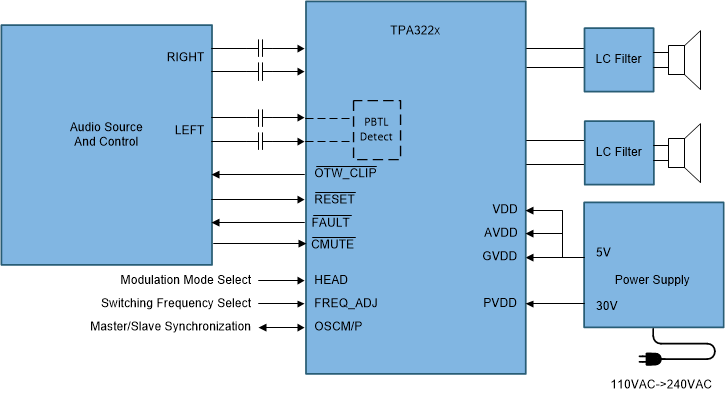
Simplified Schematic
