SLASEN3B January   2018  – August 2018 TPA3220

PRODUCTION DATA.  

  1. Features
  2. Applications
  3. Description
    1.     Simplified Schematic
  4. Revision History
  5. Device Comparison Table
  6. Pin Configuration and Functions
    1.     Pin Functions
  7. Specifications
    1. 7.1 Absolute Maximum Ratings
    2. 7.2 ESD Ratings
    3. 7.3 Recommended Operating Conditions
    4. 7.4 Thermal Information
    5. 7.5 Electrical Characteristics
    6. 7.6 Audio Characteristics (BTL)
    7. 7.7 Audio Characteristics (PBTL)
    8. 7.8 Typical Characteristics, BTL Configuration, AD-mode
    9. 7.9 Typical Characteristics, PBTL Configuration, AD-mode
  8. Parameter Measurement Information
  9. Detailed Description
    1. 9.1 Overview
    2. 9.2 Functional Block Diagrams
    3. 9.3 Feature Description
      1. 9.3.1 Internal LDO
        1. 9.3.1.1 Input Configuration, Gain Setting And Master / Slave Operation
      2. 9.3.2 Gain Setting And Master / Slave Operation
      3. 9.3.3 AD-Mode and HEAD-Mode PWM Modulation
      4. 9.3.4 Oscillator
      5. 9.3.5 Input Impedance
      6. 9.3.6 Error Reporting
    4. 9.4 Device Functional Modes
      1. 9.4.1 Powering Up
        1. 9.4.1.1 Startup Ramp Time
      2. 9.4.2 Powering Down
        1. 9.4.2.1 Power Down Ramp Time
      3. 9.4.3 Device Reset
      4. 9.4.4 Device Soft Mute
      5. 9.4.5 Device Protection System
        1. 9.4.5.1 Overload and Short Circuit Current Protection
        2. 9.4.5.2 Signal Clipping and Pulse Injector
        3. 9.4.5.3 DC Speaker Protection
        4. 9.4.5.4 Pin-to-Pin Short Circuit Protection (PPSC)
        5. 9.4.5.5 Overtemperature Protection OTW and OTE
        6. 9.4.5.6 Undervoltage Protection (UVP) and Power-on Reset (POR)
        7. 9.4.5.7 Fault Handling
  10. 10Application and Implementation
    1. 10.1 Application Information
    2. 10.2 Typical Applications
      1. 10.2.1 Stereo BTL Application
        1. 10.2.1.1 Design Requirements
        2. 10.2.1.2 Detailed Design Procedures
          1. 10.2.1.2.1 Decoupling Capacitor Recommendations
          2. 10.2.1.2.2 PVDD Capacitor Recommendation
          3. 10.2.1.2.3 BST capacitors
          4. 10.2.1.2.4 PCB Material Recommendation
      2. 10.2.2 Typical Application, Differential (2N), AD-Mode PBTL (Outputs Paralleled before LC filter)
        1. 10.2.2.1 Design Requirements
      3. 10.2.3 Typical Application, Differential (2N), AD-Mode PBTL (Outputs Paralleled after LC filter)
        1. 10.2.3.1 Design Requirements
  11. 11Power Supply Recommendations
    1. 11.1 Power Supplies
      1. 11.1.1 VDD Supply
      2. 11.1.2 AVDD and GVDD Supplies
      3. 11.1.3 PVDD Supply
      4. 11.1.4 BST Supply
  12. 12Layout
    1. 12.1 Layout Guidelines
    2. 12.2 Layout Examples
      1. 12.2.1 BTL Application Printed Circuit Board Layout Example
      2. 12.2.2 PBTL (Outputs Paralleled before LC filter) Application Printed Circuit Board Layout Example
      3. 12.2.3 PBTL (Outputs Paralleled after LC filter) Application Printed Circuit Board Layout Example
  13. 13Device and Documentation Support
    1. 13.1 Documentation Support
    2. 13.2 Receiving Notification of Documentation Updates
    3. 13.3 Community Resources
    4. 13.4 Trademarks
    5. 13.5 Electrostatic Discharge Caution
    6. 13.6 Glossary
  14. 14Mechanical, Packaging, and Orderable Information

Package Options

Refer to the PDF data sheet for device specific package drawings

Mechanical Data (Package|Pins)
  • DDW|44
Thermal pad, mechanical data (Package|Pins)
Orderable Information

Mechanical, Packaging, and Orderable Information

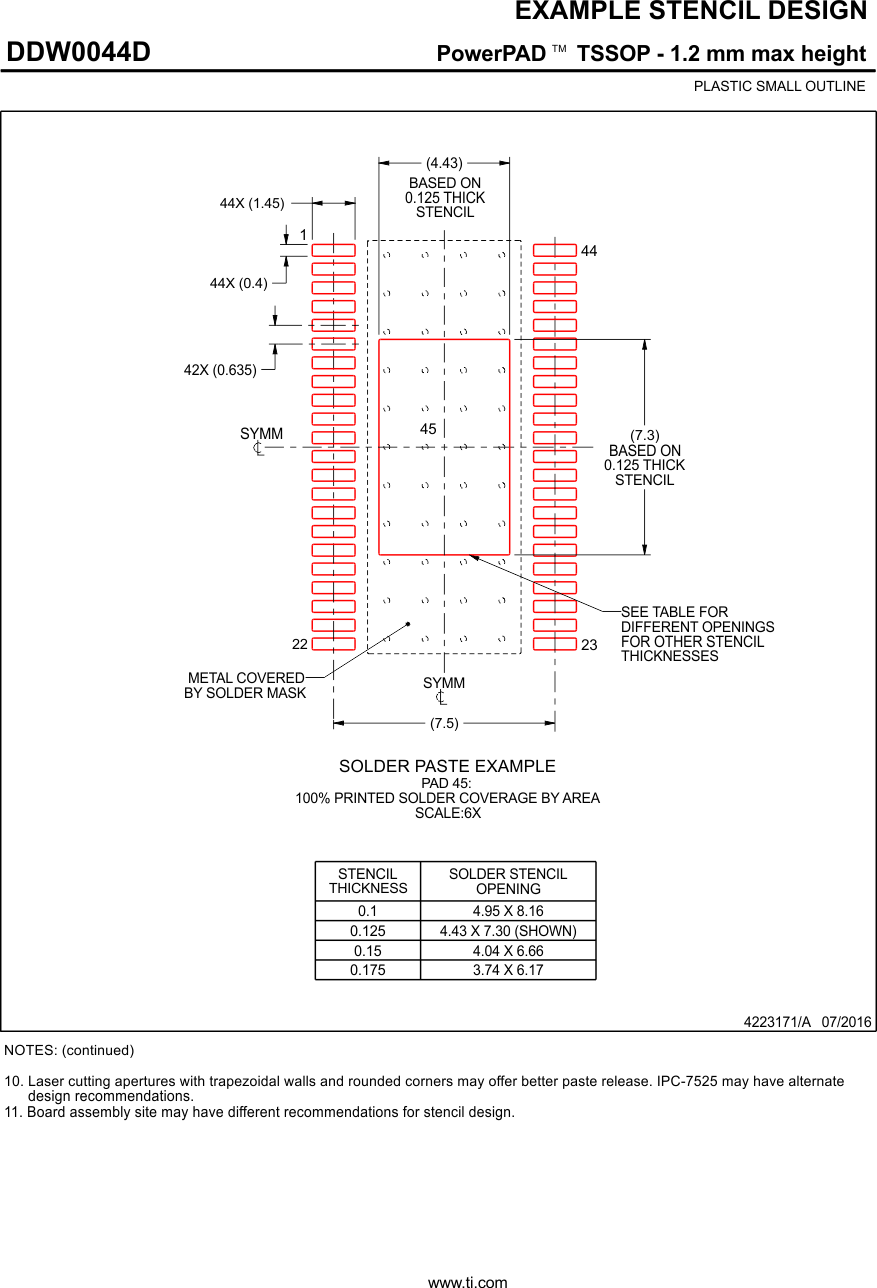
The following pages include mechanical, packaging, and orderable information. This information is the most current data available for the designated devices. This data is subject to change without notice and revision of this document. For browser-based versions of this data sheet, refer to the left-hand navigation.
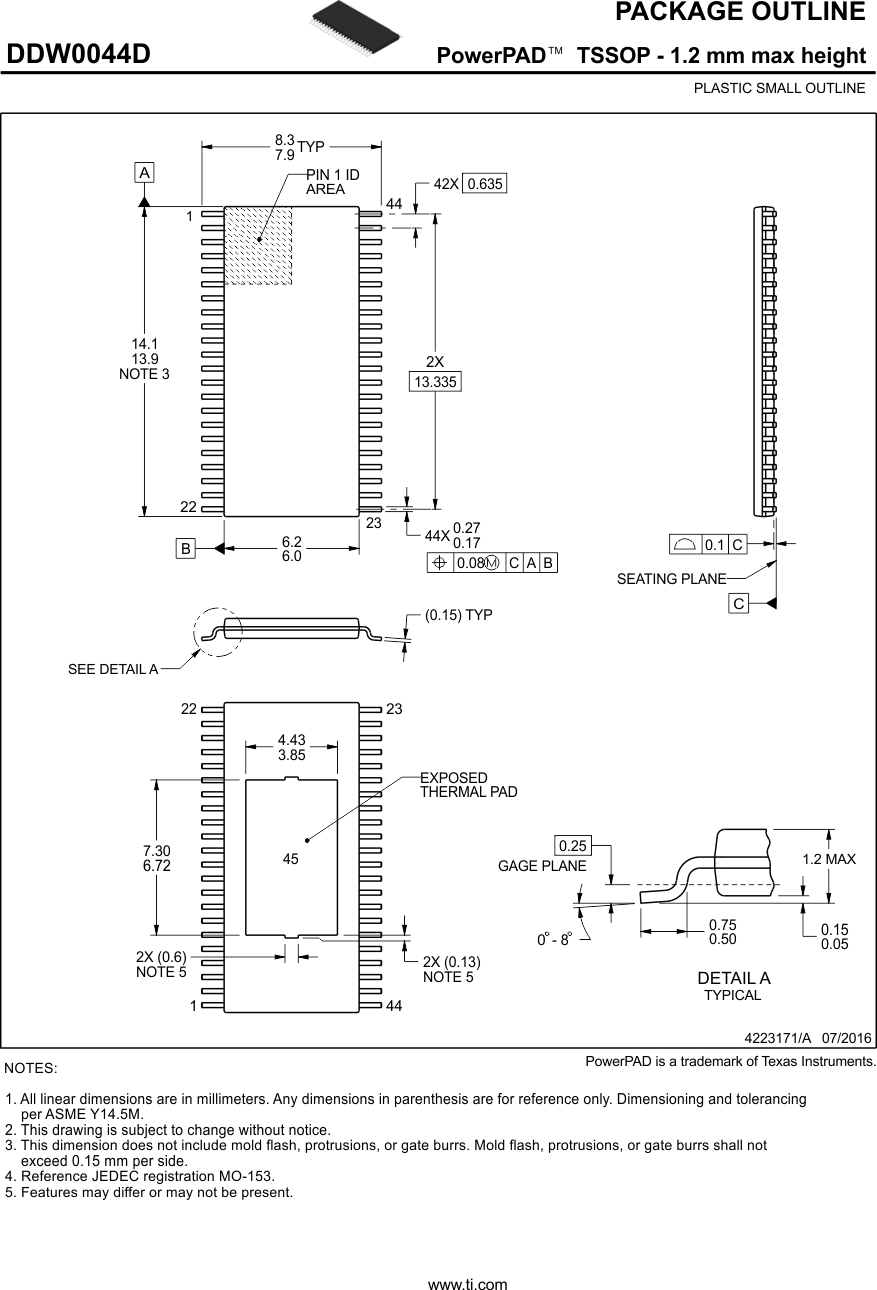
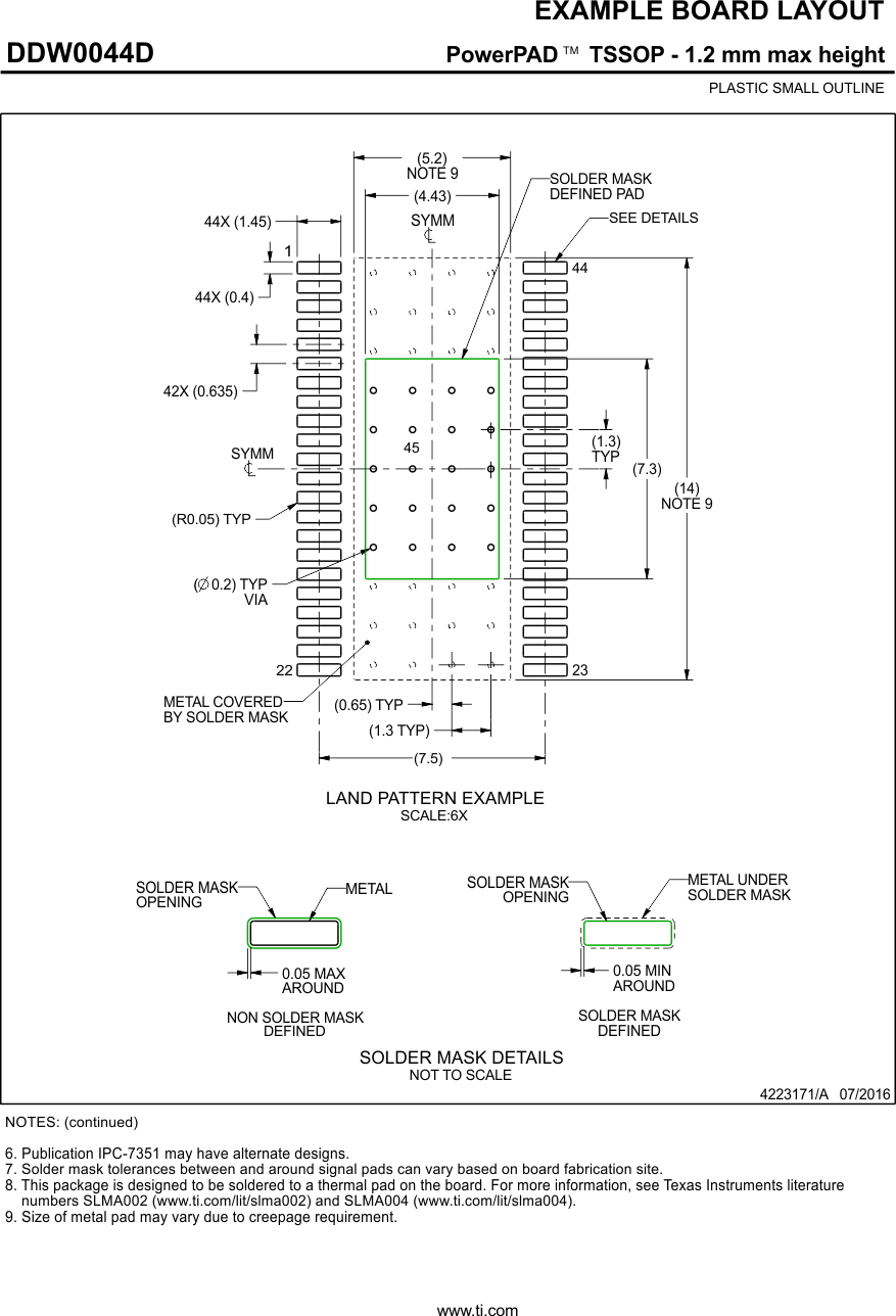
TPA3220 DDW0044D_4223171_Page_01.gif
TPA3220 DDW0044D_4223171_Page_02.gif
TPA3220 DDW0044D_4223171_Page_03.gif