SLASEN3B January 2018 – August 2018 TPA3220
PRODUCTION DATA.
- 1 Features
- 2 Applications
- 3 Description
- 4 Revision History
- 5 Device Comparison Table
- 6 Pin Configuration and Functions
-
7 Specifications
- 7.1 Absolute Maximum Ratings
- 7.2 ESD Ratings
- 7.3 Recommended Operating Conditions
- 7.4 Thermal Information
- 7.5 Electrical Characteristics
- 7.6 Audio Characteristics (BTL)
- 7.7 Audio Characteristics (PBTL)
- 7.8 Typical Characteristics, BTL Configuration, AD-mode
- 7.9 Typical Characteristics, PBTL Configuration, AD-mode
- 8 Parameter Measurement Information
-
9 Detailed Description
- 9.1 Overview
- 9.2 Functional Block Diagrams
- 9.3 Feature Description
- 9.4
Device Functional Modes
- 9.4.1 Powering Up
- 9.4.2 Powering Down
- 9.4.3 Device Reset
- 9.4.4 Device Soft Mute
- 9.4.5
Device Protection System
- 9.4.5.1 Overload and Short Circuit Current Protection
- 9.4.5.2 Signal Clipping and Pulse Injector
- 9.4.5.3 DC Speaker Protection
- 9.4.5.4 Pin-to-Pin Short Circuit Protection (PPSC)
- 9.4.5.5 Overtemperature Protection OTW and OTE
- 9.4.5.6 Undervoltage Protection (UVP) and Power-on Reset (POR)
- 9.4.5.7 Fault Handling
- 10Application and Implementation
- 11Power Supply Recommendations
- 12Layout
- 13Device and Documentation Support
- 14Mechanical, Packaging, and Orderable Information
Package Options
Refer to the PDF data sheet for device specific package drawings
Mechanical Data (Package|Pins)
- DDW|44
Thermal pad, mechanical data (Package|Pins)
Orderable Information
9.4.1 Powering Up
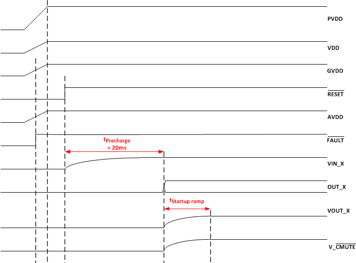
The TPA3220 does not require a power-up sequence because of the integrated undervoltage protection (UVP), but it is recommended to hold RESET low until PVDD supply voltage is stable to avoid audio artifacts. The outputs of the H-bridges remain in a high-impedance state until the gate-drive supply (GVDD) and AVDD voltages are above their UVP voltage thresholds (see the Electrical Characteristics table of this data sheet). This allows an internal circuit to charge the external bootstrap capacitors by enabling a weak pull-down of the half-bridge output as well as initiating a controlled ramp up sequence of the output voltage.
 Figure 47. Startup Timing
 When RESET is released to turn on TPA3220, FAULT signal will turn low and AVDD voltage regulator will be enabled. FAULT will stay low until AVDD reaches the undervoltage protection (UVP) voltage threshold (see the Electrical Characteristics table of this data sheet). After a pre-charge time to stabilize the DC voltage across the input AC coupling capacitors, the ramp up sequence starts and completes once the CMUTE node is charged to its final value.