SLLSEU8B March   2017  – May 2020 TPD2S703-Q1

PRODUCTION DATA.  

  1. Features
  2. Applications
  3. Description
    1.     Device Images
      1.      USB 2.0 Port With Short-to-Battery and IEC ESD Protection
  4. Revision History
  5. Pin Configuration and Functions
    1.     Pin Functions
  6. Specifications
    1. 6.1  Absolute Maximum Ratings
    2. 6.2  ESD Ratings—AEC Specification
    3. 6.3  ESD Ratings—IEC Specification
    4. 6.4  ESD Ratings—ISO Specification
    5. 6.5  Recommended Operating Conditions
    6. 6.6  Thermal Information
    7. 6.7  Electrical Characteristics
    8. 6.8  Power Supply and Supply Current Consumption Chracteristics
    9. 6.9  Timing Requirements
    10. 6.10 Typical Characteristics
  7. Parameter Measurement Information
  8. Detailed Description
    1. 8.1 Overview
    2. 8.2 Functional Block Diagram
    3. 8.3 Feature Description
      1. 8.3.1 OVP Operation
      2. 8.3.2 OVP Threshold
      3. 8.3.3 D± Clamping Voltage
    4. 8.4 Device Functional Modes
  9. Application and Implementation
    1. 9.1 Application Information
    2. 9.2 Typical Application
      1. 9.2.1 Design Requirements
        1. 9.2.1.1 Device Operation
      2. 9.2.2 Detailed Design Procedure
        1. 9.2.2.1 Common choke and Inductor for VD+ and VD-
        2. 9.2.2.2 VREF Operation
          1. 9.2.2.2.1 Mode 0
          2. 9.2.2.2.2 Mode 1
        3. 9.2.2.3 Mode 1 Enable Timing
      3. 9.2.3 Application Curves
  10. 10Power Supply Recommendations
    1. 10.1 VPWR Path
    2. 10.2 VREF Pin
  11. 11Layout
    1. 11.1 Layout Guidelines
    2. 11.2 Layout Example
  12. 12Device and Documentation Support
    1. 12.1 Documentation Support
      1. 12.1.1 Related Documentation
    2. 12.2 Receiving Notification of Documentation Updates
    3. 12.3 Support Resources
    4. 12.4 Trademarks
    5. 12.5 Electrostatic Discharge Caution
    6. 12.6 Glossary
  13. 13Mechanical, Packaging, and Orderable Information

Package Options

Mechanical Data (Package|Pins)
Thermal pad, mechanical data (Package|Pins)
Orderable Information

Typical Characteristics

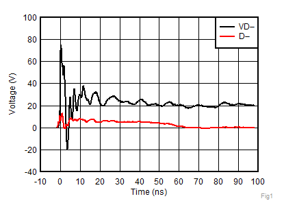
TPD2S703-Q1 Fig1_SLLSEU8.gif
Figure 2. 8-kV IEC 61400-4-2 Contact Waveform
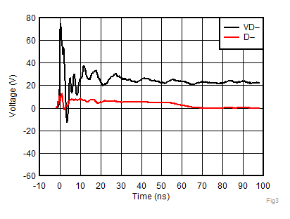
TPD2S703-Q1 Fig3_SLLSEU8.gif
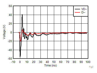
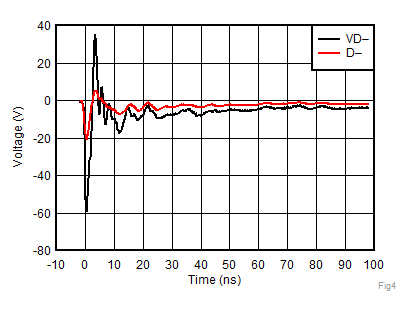
Figure 4. 8-kV ISO 10605 (330-pF, 330-Ω) Contact Waveform
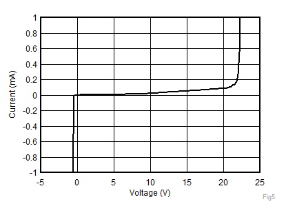
TPD2S703-Q1 Fig5_SLLSEU8.gif
Figure 6. Data Line I-V Curve
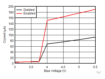
TPD2S703-Q1 Fig7_SLLSEU8.gif
Figure 8. VPWR Operating Current vs Bias Voltage
TPD2S703-Q1 D010_SLLSEU8.gif
Figure 10. VD± Leakage Current at 18 V Across Temperature (Enabled)
TPD2S703-Q1 D011_SLLSEU8.gif
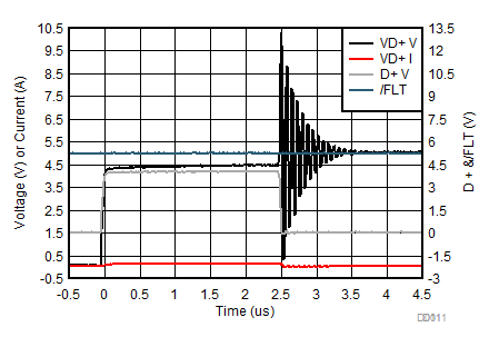
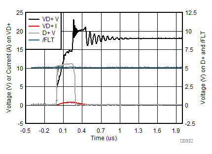
Figure 12. Data Switch Short-to-5 V Response Waveform
TPD2S703-Q1 Fig13_SLLSEU8.gif
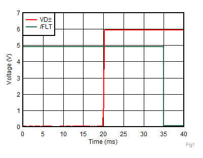
Figure 14. FLT Assertion Time During OVP
TPD2S703-Q1 D015_SLLSEU8.gif
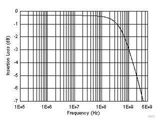
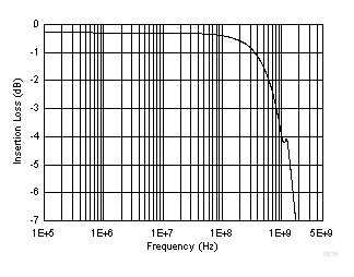
Figure 16. Data Switch Differential Bandwidth
TPD2S703-Q1 D018_SLLSEU8.gif
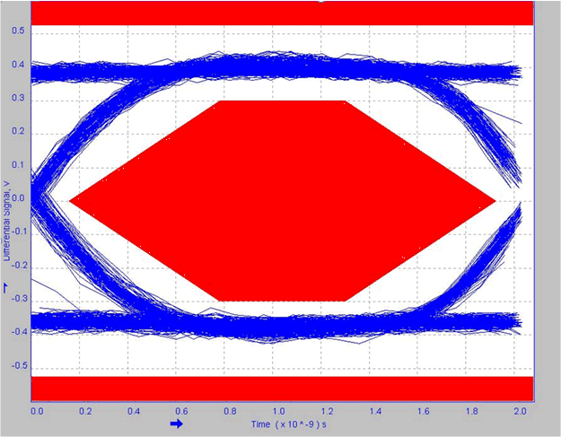
Figure 18. USB2.0 Eye Diagram (No TPD2S703-Q1)
TPD2S703-Q1 Fig2_SLLSEU8.gif
Figure 3. –8-kV IEC 61400-4-2 Contact Waveform
TPD2S703-Q1 Fig4_SLLSEU8.gif
Figure 5. –8-kV ISO 10605 (330-pF, 330-Ω) Contact Waveform
TPD2S703-Q1 Fig6_SLLSEU8.gif
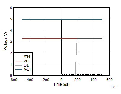
Figure 7. Data Switch Turnon Time
TPD2S703-Q1 Fig8_SLLSEU8.gif
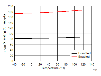
Figure 9. VPWR Operating Current vs Temperature
(VPWR = 5 V)
TPD2S703-Q1 Fig10_SLLSEU8.gif
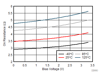
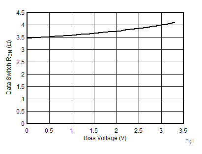
Figure 11. Data Switch RON vs Bias Voltage
TPD2S703-Q1 D012_SLLSEU8.gif
Figure 13. Data Switch Short-to-18 V Response Waveform
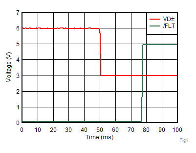
TPD2S703-Q1 Fig14_SLLSEU8.gif
Figure 15. FLT Recover Time After OVP Clear
TPD2S703-Q1 D016_SLLSEU8.gif
Figure 17. Data Switch Single-Ended Bandwidth
TPD2S703-Q1 D019_SLLSEU8.gif
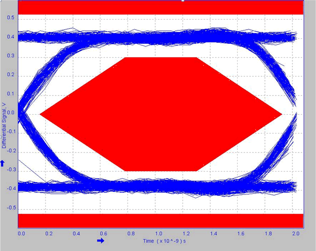
Figure 19. USB2.0 Eye Diagram (With TPD2S703-Q1)