SLIS113E October   2004  – May 2022 TPIC1021

PRODUCTION DATA  

  1. Features
  2. Applications
  3. Description
  4. Revision History
  5. Description (continued)
  6. Pin Configuration and Functions
  7. Specifications
    1. 7.1 Absolute Maximum Ratings
    2. 7.2 ESD Ratings
    3. 7.3 Recommended Operating Conditions
    4. 7.4 Thermal Information
    5. 7.5 Electrical Characteristics
    6. 7.6 Timing Requirements
    7. 7.7 Typical Characteristics
  8. Detailed Description
    1. 8.1 Overview
    2. 8.2 Functional Block Diagram
    3. 8.3 Feature Description
      1. 8.3.1 LIN Bus Pin
        1. 8.3.1.1 Transmitter Characteristics
        2. 8.3.1.2 Receiver Characteristics
      2. 8.3.2 Transmit Input Pin (TXD)
        1. 8.3.2.1 TXD Dominant State Timeout
      3. 8.3.3 Receive Output Pin (RXD)
        1. 8.3.3.1 RXD Wake-up Request
      4. 8.3.4 Ground (GND)
      5. 8.3.5 Enable Input Pin (EN)
      6. 8.3.6 NWake Input Pin (NWake)
      7. 8.3.7 Inhibit Output Pin (INH)
    4. 8.4 Device Functional Modes
      1. 8.4.1 Operating States
        1. 8.4.1.1 Normal Mode
        2. 8.4.1.2 Low Power Mode
        3. 8.4.1.3 Wake-Up Events
        4. 8.4.1.4 Standby Mode
      2. 8.4.2 Supply Voltage (VSUP)
  9. Application and Implementation
    1. 9.1 Application Information
    2. 9.2 Typical Application
      1. 9.2.1 Design Requirements
      2. 9.2.2 Detailed Design Procedure
      3. 9.2.3 Application Curves
    3. 9.3 Power Supply Recommendations
    4. 9.4 Layout
      1. 9.4.1 Layout Guidelines
      2. 9.4.2 Layout Example
  10. 10Device and Documentation Support
    1. 10.1 Receiving Notification of Documentation Updates
    2. 10.2 Support Resources
    3. 10.3 Trademarks
    4. 10.4 Electrostatic Discharge Caution
    5. 10.5 Glossary
  11. 11Mechanical, Packaging, and Orderable Information

Package Options

Refer to the PDF data sheet for device specific package drawings

Mechanical Data (Package|Pins)
  • D|8
Thermal pad, mechanical data (Package|Pins)
Orderable Information

Description

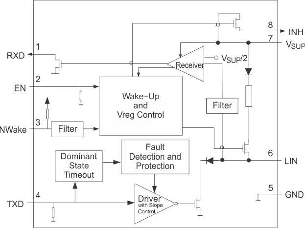
The TPIC1021 is the LIN (Local Interconnect Network) physical interface, which integrates the serial transceiver with wake up and protection features. The LIN bus is a single wire, bi-directional bus typically used for low-speed in-vehicle networks using baud rates between 2.4 kbps and 20 kbps.

The LIN bus has two logical values: the dominant state (voltage near ground) represents a logic 0 and the recessive state (voltage near battery) and represents logic 1.

In the recessive state, the LIN bus is pulled high by the TPIC1021 internal pull-up resistor (30 kΩ) and series diode, so no external pullup components are required for responder applications. Commander applications require an external pullup resistor (1 kΩ) plus a series diode.

Device Information
PART NUMBERPACKAGE(1)BODY SIZE (NOM)
TPIC1021SOIC (8)4.90 mm × 3.91 mm
For all available packages, see the orderable addendum at the end of the data sheet.
GUID-53E306D5-3FE0-4D92-A825-3A68DC6171C0-low.gifFunctional Block Diagram