SLVSB97E July 2012 – January 2018 TPS23751 , TPS23752
PRODUCTION DATA.
- 1 Features
- 2 Applications
- 3 Description
- 4 Revision History
- 5 Pin Configuration and Functions
-
6 Specifications
- 6.1 Absolute Maximum Ratings
- 6.2 ESD Ratings
- 6.3 ESD Ratings: Surge
- 6.4 Recommended Operating Conditions
- 6.5 Thermal Information
- 6.6 Electric Characteristics - Controller Section
- 6.7 Electrical Characteristics - Sleep Mode (TPS23752 Only)
- 6.8 Electrical Characteristics - PoE Interface Section
- 6.9 Typical Characteristics
-
7 Detailed Description
- 7.1 Overview
- 7.2 Functional Block Diagrams
- 7.3 Feature Description
- 7.4
Device Functional Modes
- 7.4.1 PoE Overview
- 7.4.2
Sleep Mode Operation (TPS23752 only)
- 7.4.2.1 Converter Controller Features
- 7.4.2.2 PWM and VFO Operation; CTL, SRT, and SRD Pin Relationships to Output Load Current
- 7.4.2.3 Bootstrap Topology
- 7.4.2.4 Current Slope Compensation and Current Limit
- 7.4.2.5 RT
- 7.4.2.6 T2P, Startup and Power Management
- 7.4.2.7 Thermal Shutdown
- 7.4.2.8 Adapter ORing
- 7.4.2.9 Using DEN to Disable PoE
- 7.4.2.10 ORing Challenges
-
8 Application and Implementation
- 8.1 Application Information
- 8.2
Typical Application
- 8.2.1 Design Requirements
- 8.2.2
Detailed Design Procedure
- 8.2.2.1 Input Bridges and Schottky Diodes
- 8.2.2.2 Protection, D1
- 8.2.2.3 Capacitor, C1
- 8.2.2.4 Detection Resistor, RDEN
- 8.2.2.5 Classification Resistor, RCLS
- 8.2.2.6 APD Pin Divider Network, RAPD1, RAPD2
- 8.2.2.7 Setting the PWM-VFO Threshold using the SRT pin
- 8.2.2.8 Setting Frequency (RT)
- 8.2.2.9 Current Slope Compensation
- 8.2.2.10 Voltage Feed-Forward Compensation
- 8.2.2.11 Estimating Bias Supply Requirements and Cvc
- 8.2.2.12 Switching Transformer Considerations and RVC
- 8.2.2.13 T2P Pin Interface
- 8.2.2.14 Softstart
- 8.2.2.15 Special Switching MOSFET Considerations
- 8.2.2.16 ESD
- 8.2.2.17 Thermal Considerations and OTSD
- 8.2.3 Application Curves
- 9 Power Supply Recommendations
- 10Layout
- 11Device and Documentation Support
- 12Mechanical, Packaging, and Orderable Information
Package Options
Mechanical Data (Package|Pins)
- PWP|20
Thermal pad, mechanical data (Package|Pins)
- PWP|20
Orderable Information
8.2.2.9 Current Slope Compensation
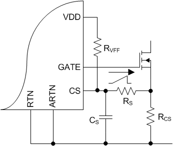
The TPS23751 and TPS23752 provide a fixed internal compensation ramp that suffices for most applications. RS (see Figure 32) may be used if the internally provided slope compensation is not enough. Most current-mode control papers and application notes define the slope values in terms of VPP/TS (peak ramp voltage / switching period). Assuming that the desired slope, VSLOPE_D (in mV/period), as shown in Figure 1, is based on the full period, compute RS per the following equation where VPK and ICS_RAMP are from the electrical characteristics table with voltages in mV and current in μA.

 Figure 32. Additional Slope Compensation
CS may be required if the presence of RS causes increased noise, due to adjacent signals like the gate drive, to appear at the CS pin.