SLVSB97E July 2012 – January 2018 TPS23751 , TPS23752
PRODUCTION DATA.
- 1 Features
- 2 Applications
- 3 Description
- 4 Revision History
- 5 Pin Configuration and Functions
-
6 Specifications
- 6.1 Absolute Maximum Ratings
- 6.2 ESD Ratings
- 6.3 ESD Ratings: Surge
- 6.4 Recommended Operating Conditions
- 6.5 Thermal Information
- 6.6 Electric Characteristics - Controller Section
- 6.7 Electrical Characteristics - Sleep Mode (TPS23752 Only)
- 6.8 Electrical Characteristics - PoE Interface Section
- 6.9 Typical Characteristics
-
7 Detailed Description
- 7.1 Overview
- 7.2 Functional Block Diagrams
- 7.3 Feature Description
- 7.4
Device Functional Modes
- 7.4.1 PoE Overview
- 7.4.2
Sleep Mode Operation (TPS23752 only)
- 7.4.2.1 Converter Controller Features
- 7.4.2.2 PWM and VFO Operation; CTL, SRT, and SRD Pin Relationships to Output Load Current
- 7.4.2.3 Bootstrap Topology
- 7.4.2.4 Current Slope Compensation and Current Limit
- 7.4.2.5 RT
- 7.4.2.6 T2P, Startup and Power Management
- 7.4.2.7 Thermal Shutdown
- 7.4.2.8 Adapter ORing
- 7.4.2.9 Using DEN to Disable PoE
- 7.4.2.10 ORing Challenges
-
8 Application and Implementation
- 8.1 Application Information
- 8.2
Typical Application
- 8.2.1 Design Requirements
- 8.2.2
Detailed Design Procedure
- 8.2.2.1 Input Bridges and Schottky Diodes
- 8.2.2.2 Protection, D1
- 8.2.2.3 Capacitor, C1
- 8.2.2.4 Detection Resistor, RDEN
- 8.2.2.5 Classification Resistor, RCLS
- 8.2.2.6 APD Pin Divider Network, RAPD1, RAPD2
- 8.2.2.7 Setting the PWM-VFO Threshold using the SRT pin
- 8.2.2.8 Setting Frequency (RT)
- 8.2.2.9 Current Slope Compensation
- 8.2.2.10 Voltage Feed-Forward Compensation
- 8.2.2.11 Estimating Bias Supply Requirements and Cvc
- 8.2.2.12 Switching Transformer Considerations and RVC
- 8.2.2.13 T2P Pin Interface
- 8.2.2.14 Softstart
- 8.2.2.15 Special Switching MOSFET Considerations
- 8.2.2.16 ESD
- 8.2.2.17 Thermal Considerations and OTSD
- 8.2.3 Application Curves
- 9 Power Supply Recommendations
- 10Layout
- 11Device and Documentation Support
- 12Mechanical, Packaging, and Orderable Information
Package Options
Mechanical Data (Package|Pins)
- PWP|20
Thermal pad, mechanical data (Package|Pins)
- PWP|20
Orderable Information
6.8 Electrical Characteristics - PoE Interface Section
Unless otherwise noted, 40 V ≤ VDD ≤ 57 V; VCTL = VMODE = VSLPb = VB; VSRT = 0.5 V; VAPD = VCS = VARTN = VRTN; CLS, GATE, LED, SRD, T2P open; RWAKE = 392 kΩ; RDEN = 24.9 kΩ; RT = 34 kΩ; CVB = CVC = 0.1 µF;–40 ≤ TJ ≤ 125°C. Typical values are at 25°C. All voltages referred to VSS.
Unless otherwise noted, VVC = VAPD = VCS = VARTN = VRTN.
| PARAMETER | TEST CONDITIONS | MIN | TYP | MAX | UNIT | |
|---|---|---|---|---|---|---|
| DEN (DETECTION AND ENABLE) | ||||||
| Bias current | DEN open, IVDD + IDEN + IRTN, VVDD = 10.1 V, not in mark | 3 | 5 | 12 | µA | |
| DEN leakage current | VDEN = VVDD = 57 V | 0.1 | 5 | µA | ||
| Detection current | IVDD + IDEN + IRTN, VVDD = 1.4 V | 53.8 | 56.5 | 58.3 | µA | |
| IVDD + IDEN + IRTN, VVDD = 10.1 V | 395 | 410 | 417 | |||
| VPD_DIS | Disable threshold | DEN falling | 3 | 3.6 | 5 | V |
| Hysteresis | 50 | 113 | 200 | mV | ||
| CLS (CLASSIFICATION) | ||||||
| ICLS | Classification current | 13 V ≤ VVDD ≤ 21 V, Measure IVDD + IDEN + IRTN | mA | |||
| RCLS = 1270 Ω | 1.80 | 2.17 | 2.60 | |||
| RCLS = 243 Ω | 9.90 | 10.60 | 11.20 | |||
| RCLS = 137 Ω | 17.60 | 18.60 | 19.40 | |||
| RCLS = 90.9 Ω | 26.50 | 27.90 | 29.30 | |||
| RCLS = 63.4 Ω | 38.00 | 39.90 | 42.00 | |||
| VCL_ON VCL_H |
Class lower threshold | VVDD rising, VCLS ↑ | 11.9 | 12.5 | 13 | V |
| Hysteresis | 1.4 | 1.6 | 1.7 | V | ||
| VCU_OFF VCU_H |
Class upper threshold | VVDD rising, VCLS ↓ | 21 | 22 | 23 | V |
| Hysteresis | 0.50 | 0.75 | 0.90 | V | ||
| VMSR | Mark reset threshold | VVDD falling | 3 | 3.9 | 5 | V |
| Mark state resistance | 2-point measurement at 5 V and 10.1 V | 6 | 9.1 | 12 | kΩ | |
| Leakage current | VVDD = 57 V, VCLS = 0 V, measure ICLS | 1 | µA | |||
| RTN (PASS DEVICE) | ||||||
| rDS(on) | On resistance | VVC = VAPD = VARTN = VCS = VVDD | 0.20 | 0.45 | 0.75 | Ω |
| Current limit | VVC = VAPD = VARTN = VCS = VVDD, VRTN =1.5 V, Measure IRTN | 0.85 | 1.00 | 1.20 | A | |
| Inrush current | VVC = VAPD = VARTN = VCS = VDD, VRTN = 2 V, VDD = 20 V → 48 V | 100 | 140 | 180 | mA | |
| Inrush termination | Percentage of inrush current | 80% | 90% | 99% | ||
| Foldback threshold | VRTN ↑ | 11.0 | 12.3 | 13.6 | V | |
| Foldback deglitch time | VRTN rising to when current limit changes to inrush current limit | 500 | 800 | 1500 | µs | |
| Input bias current | VVDD = VRTN = 30 V, Measure IRTN | 30 | µA | |||
| RTN leakage current | VRTN = VVDD = 100 V, VDEN = VVSS | 50 | µA | |||
| T2P (TYPE 2 PSE INDICATION) | ||||||
| VT2P | Output low voltage | IT2P = 2 mA, after 2-event classification and softstart is complete, VVC = 12 V, VCTL = 3 V, VARTN = VVSS |
0.26 | 0.60 | V | |
| tT2P | T2P startup delay | VCTL = 3 V, VAPD = 2 V, Measure from switching start to VT2P ↓ | 2 | 4.3 | 7 | ms |
| Leakage current | VT2P = 18 V, VARTN = VVSS | 10 | µA | |||
| PoE – PD UVLO | ||||||
| VUVLO_R | UVLO rising threshold | 36.3 | 38.1 | 40 | V | |
| UVLO falling threshold | 30.5 | 32.0 | 33.6 | |||
| SUPPLY CURRENT | ||||||
| Operating current | Measure IVDD, VVDD = 48 V, 40 V ≤ VVDD ≤ 57 V | 210 | 500 | µA | ||
| Off-state current | ARTN and VVC open, VVDD = 30 V, Measure IVDD | 300 | µA | |||
| THERMAL SHUTDOWN | ||||||
| Shutdown | TJ rising | 135 | 145 | 155 | °C | |
| Hysteresis (1) | 20 | °C | ||||
(1) Parameters provided for reference only, and do not constitute part of TI published specifications for purposes of TI product warranty.
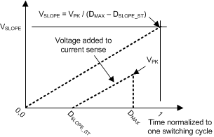
 Figure 1. Current Mode Compensation Ramp
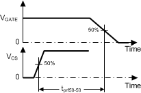
 Figure 2. Time Delay from VCS to VGATE
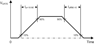
 Figure 3. Rise Time and Fall Time of VGATE