SLVSB97E July 2012 – January 2018 TPS23751 , TPS23752
PRODUCTION DATA.
- 1 Features
- 2 Applications
- 3 Description
- 4 Revision History
- 5 Pin Configuration and Functions
-
6 Specifications
- 6.1 Absolute Maximum Ratings
- 6.2 ESD Ratings
- 6.3 ESD Ratings: Surge
- 6.4 Recommended Operating Conditions
- 6.5 Thermal Information
- 6.6 Electric Characteristics - Controller Section
- 6.7 Electrical Characteristics - Sleep Mode (TPS23752 Only)
- 6.8 Electrical Characteristics - PoE Interface Section
- 6.9 Typical Characteristics
-
7 Detailed Description
- 7.1 Overview
- 7.2 Functional Block Diagrams
- 7.3 Feature Description
- 7.4
Device Functional Modes
- 7.4.1 PoE Overview
- 7.4.2
Sleep Mode Operation (TPS23752 only)
- 7.4.2.1 Converter Controller Features
- 7.4.2.2 PWM and VFO Operation; CTL, SRT, and SRD Pin Relationships to Output Load Current
- 7.4.2.3 Bootstrap Topology
- 7.4.2.4 Current Slope Compensation and Current Limit
- 7.4.2.5 RT
- 7.4.2.6 T2P, Startup and Power Management
- 7.4.2.7 Thermal Shutdown
- 7.4.2.8 Adapter ORing
- 7.4.2.9 Using DEN to Disable PoE
- 7.4.2.10 ORing Challenges
-
8 Application and Implementation
- 8.1 Application Information
- 8.2
Typical Application
- 8.2.1 Design Requirements
- 8.2.2
Detailed Design Procedure
- 8.2.2.1 Input Bridges and Schottky Diodes
- 8.2.2.2 Protection, D1
- 8.2.2.3 Capacitor, C1
- 8.2.2.4 Detection Resistor, RDEN
- 8.2.2.5 Classification Resistor, RCLS
- 8.2.2.6 APD Pin Divider Network, RAPD1, RAPD2
- 8.2.2.7 Setting the PWM-VFO Threshold using the SRT pin
- 8.2.2.8 Setting Frequency (RT)
- 8.2.2.9 Current Slope Compensation
- 8.2.2.10 Voltage Feed-Forward Compensation
- 8.2.2.11 Estimating Bias Supply Requirements and Cvc
- 8.2.2.12 Switching Transformer Considerations and RVC
- 8.2.2.13 T2P Pin Interface
- 8.2.2.14 Softstart
- 8.2.2.15 Special Switching MOSFET Considerations
- 8.2.2.16 ESD
- 8.2.2.17 Thermal Considerations and OTSD
- 8.2.3 Application Curves
- 9 Power Supply Recommendations
- 10Layout
- 11Device and Documentation Support
- 12Mechanical, Packaging, and Orderable Information
Package Options
Mechanical Data (Package|Pins)
- PWP|20
Thermal pad, mechanical data (Package|Pins)
- PWP|20
Orderable Information
7.4.1.4 Hardware Classification
Hardware classification allows a PSE to determine the power requirements of a PD before powering, and helps with power management once power is applied. Type 2 hardware classification permits high power PSEs and PDs to determine whether the connected device can support high-power operation. A type 2 PD presents class 4 in hardware to indicate that it is a high-power device. A type 1 PSE treats a class 4 device like a class 0 device, allotting 13 W if it chooses to power the PD. A PD that receives a 2-event class understands that it is powered from a high-power PSE and it may draw up to 25.5 W immediately after the 80 ms startup period completes. A type 2 PD that does not receive a 2-event hardware classification may choose to not start, or must start in a 13 W condition and request more power through the DLL after startup. The standard requires a type 2 PD to indicate that it is underpowered if this occurs. Startup of a high-power PD under 13 W implicitly requires some form of powering down sections of the application circuits.
The maximum power entries in Table 1 determine the class the PD must advertise. The PSE may disconnect a PD if it draws more than its stated Class power, which may be the hardware class or a lower DLL-derived power level. The standard permits the PD to draw limited current peaks that increase the instantaneous power above the Table 1 limit, however the average power requirement always applies.
The TPS23751 and TPS23752 implement two-event classification. Selecting an RCLS of 63.4 Ω provides a valid type 2 signature. A TPS23751 or TPS23752 may be used as a compatible type 1 device simply by programming class 0–3 per Table 1. DLL communication is implemented by the Ethernet communication system in the PD and is not implemented by the TPS23751 or TPS23752.
The TPS23751 and TPS23752 disable classification above VCU_OFF to avoid excessive power dissipation. CLS voltage is turned off during PD thermal limiting or when DEN is active. The CLS output is inherently current limited, but should not be shorted to VSS for long periods of time.
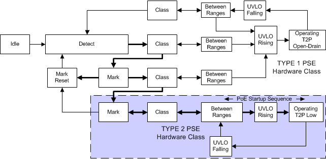
Figure 25 shows how classification works for the TPS23751 and TPS23752. Transition from state-to-state occurs when comparator thresholds are crossed (see Figure 22 and Figure 23). These comparators have hysteresis, which adds inherent memory to the machine. Operation begins at idle (unpowered by PSE) and proceeds with increasing voltage from left to right. A 2-event classification follows the (heavy lined) path towards the bottom, ending up with a latched type 2 decode along the lower branch that is highlighted. This state results in a low T2P during normal operation. Once the valid path to type 2 PSE detection is broken, the input voltage must transition below the mark reset threshold to start anew.
 Figure 25. Two-Event Class Internal States