SLVS727E November 2006 – October 2019 TPS2410 , TPS2411
PRODUCTION DATA.
- 1 Features
- 2 Applications
- 3 Description
- 4 Revision History
- 5 Device Comparison
- 6 Pin Configuration and Functions
- 7 Specifications
- 8 Detailed Description
- 9 Application and Implementation
- 10Power Supply Recommendations
- 11Layout
- 12Device and Documentation Support
- 13Mechanical, Packaging, and Orderable Information
Package Options
Mechanical Data (Package|Pins)
Thermal pad, mechanical data (Package|Pins)
Orderable Information
8.3.3 Fast Comparator Input Filtering – C(FLTR)
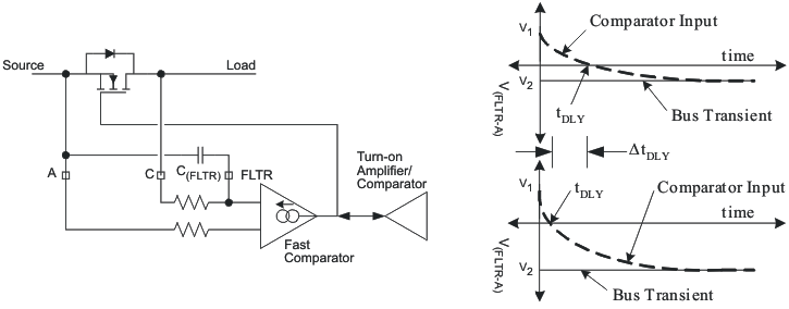
The FLTR (filter) pin enables a simple method of filtering the input to the fast turn-off comparator as demonstrated in Figure 6. To minimize the impact of a bus fault, the ORing controller turns off the external MOSFET as fast as possible when a voltage reversal occurs. However, having a fast reaction increases the likelihood that noise or non-fault transients may cause false triggering. Examples of such transients are ESD, EFT, RF induction, step loads, and insertion of high-inrush units. The effect of the filter on a time-domain transient are illustrated by assuming a step input from positive to negative. The expression for the time to reach 0 V across the fast comparator inputs follows, where the variables are defined in Figure 6.

Figure 6 graphically illustrates that the external MOSFET is turned off after a longer delay for a small transient than a large voltage reversal. For example, the delay from 10 mV forward to 10-mV reverse is about 52 ns (R = 520 Ω, C = 150 pF), while the delay for a 100-mV reverse transient is 7 ns. It is unlikely that the transient in a real system is a step response, making exact calculations on the effect of the R-C filter to a specific transient difficult.
The need for a C(FLTR), and its value, is dependent on the electrical noise environment of the particular system. If the electrical environment is understood, the need for the filter, or its value, is selected based on approximations or simulations. If the system is not understood or does not exist when the TPS2410 circuit design is completed, it is recommended that a C(FLTR) of 100 pF be included in initial schematics. Evaluation of system performance may allow removal of C(FLTR). The tolerance of the internal resistance is about ±25% including temperature variations.
 Figure 6. Fast Comparator Input Filtering