SLVS727E November 2006 – October 2019 TPS2410 , TPS2411
PRODUCTION DATA.
- 1 Features
- 2 Applications
- 3 Description
- 4 Revision History
- 5 Device Comparison
- 6 Pin Configuration and Functions
- 7 Specifications
- 8 Detailed Description
- 9 Application and Implementation
- 10Power Supply Recommendations
- 11Layout
- 12Device and Documentation Support
- 13Mechanical, Packaging, and Orderable Information
Package Options
Mechanical Data (Package|Pins)
Thermal pad, mechanical data (Package|Pins)
Orderable Information
8.3.5 Input ORing and Stat
STAT provides information regarding the state of the MOSFET gate drive. STAT is pulled to VDD, through a 46-kΩ internal pullup, if GATE is being driven high and V(GATE) exceeds V(A) plus 0.4 V. The STAT pin may be directly connected to low-voltage logic by using the logic gate input ESD clamp to control the voltage or by using a much lower pullup resistor (that is, 5 kΩ) to the logic supply voltage. STAT must be allowed to rise above VDD/2 to avoid effecting the reverse turn-off threshold.
Interconnecting STAT pins can be used to reduce the occurrence of both MOSFETs turning off in topologies such as Figure 11 that normally have both MOSFETs ON. This might occur when there is a noise transient on both buses due to fans cycling on and off, or an ac mains disturbance. If both MOSFETs are ON, and then an ORing circuit turns OFF, the second ORing circuit fast turnoff threshold is shifted negative by 157 mV from the RSET programmed value because STAT is pulled low. This reduces the probability that it too turns off as the arrival of the transient, and speed of both circuits, is unlikely to be matched. Maintaining at least one device ON avoids both a bus transient due to the current interruption, and momentary downstream hotswap overload when the ORing recovers. The function of STAT is not limited to the topology of Figure 11 and may be used to dynamically shift the fast turnoff threshold. The internal circuit shown in the FUNCTIONAL BLOCK DIAGRAM assists in designing these applications.
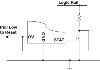
Figure 8 shows how STAT and OV can be used to latch the TPS2410 off. This is useful when a system operation benefits from preventing a failed power module from repeatedly disturbing the bus, and may be used in conjunction with back-to-back MOSFETs. The OV pin must be help low until V(GATE) is 0.4 V above V(A) in order to accomplish a reset.
 Figure 8. Use of STAT and OV to Latch TPS2411 OFF