SLVS331J December   2000  – August 2024 TPS3813

PRODUCTION DATA  

  1.   1
  2. Features
  3. Applications
  4. Description
  5. Device Comparison Table
  6. Pin Configuration and Functions
  7. Specifications
    1. 6.1 Absolute Maximum Ratings
    2. 6.2 ESD Ratings
    3. 6.3 Recommended Operating Conditions
    4. 6.4 Thermal Information
    5. 6.5 Electrical Characteristics
    6. 6.6 Timing Requirements
    7. 6.7 Switching Characteristics
    8. 6.8 Dissipation Ratings
    9. 6.9 Typical Characteristics
  8. Detailed Description
    1. 7.1 Overview
    2. 7.2 Functional Block Diagram
    3. 7.3 Feature Description
      1. 7.3.1 Input Voltage (VDD)
        1. 7.3.1.1 VDD Hysteresis
        2. 7.3.1.2 VDD Glitch Immunity
      2. 7.3.2 User-Programmable Watchdog Timer (WDI)
      3. 7.3.3 RESET Output
    4. 7.4 Device Functional Modes
      1. 7.4.1 Normal Operation (VDD > VIT)
      2. 7.4.2 Above Power-On Reset But Less Than Threshold (VPOR < VDD < VIT)
      3. 7.4.3 Below Power-On Reset (VDD < VPOR)
    5. 7.5 Programming
      1. 7.5.1 Implementing Window-Watchdog Settings
      2. 7.5.2 Programmable Window-Watchdog by Using an External Capacitor
      3. 7.5.3 Lower Boundary Calculation
      4. 7.5.4 Watchdog Software Considerations
      5. 7.5.5 Power-Up Considerations
  9. Application and Implementation
    1. 8.1 Application Information
    2. 8.2 Typical Application
      1. 8.2.1 Design Requirements
      2. 8.2.2 Detailed Design Procedure
      3. 8.2.3 Application Curve
    3. 8.3 Power Supply Recommendations
    4. 8.4 Layout
      1. 8.4.1 Layout Guidelines
      2. 8.4.2 Layout Example
  10. Device and Documentation Support
    1. 9.1 Related Links
    2. 9.2 Receiving Notification of Documentation Updates
    3. 9.3 Support Resources
    4. 9.4 Trademarks
    5. 9.5 Electrostatic Discharge Caution
    6. 9.6 Glossary
  11. 10Revision History
  12. 11Mechanical, Packaging, and Orderable Information

Package Options

Mechanical Data (Package|Pins)
Thermal pad, mechanical data (Package|Pins)
Orderable Information

Typical Characteristics

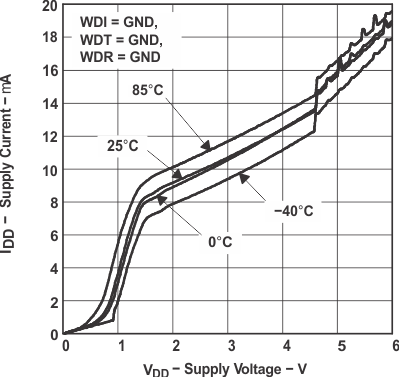
TPS3813 Supply Current vs Supply Voltage
Figure 6-2 Supply Current vs Supply Voltage
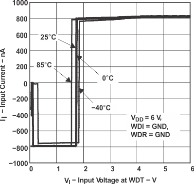
TPS3813 Input Current vs Input Voltage at WDT
Figure 6-4 Input Current vs Input Voltage at WDT
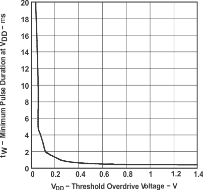
TPS3813 Minimum Pulse Duration at VDD vs VDD Threshold Overdrive Voltage
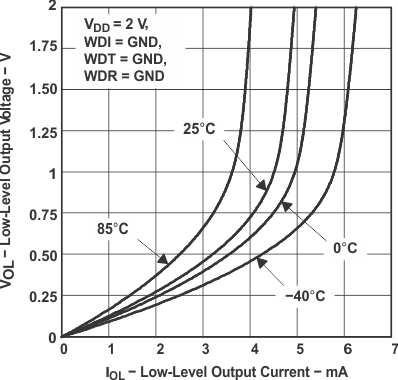
Figure 6-6 Minimum Pulse Duration at VDD vs VDD Threshold Overdrive Voltage
TPS3813 Low-Level Output Voltage vs Low-Level Output Current
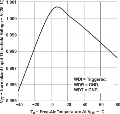
Figure 6-3 Low-Level Output Voltage vs Low-Level Output Current
TPS3813 Normalized Input Threshold Voltage vs Free-Air Temperature at VDD
Figure 6-5 Normalized Input Threshold Voltage vs Free-Air Temperature at VDD