SLVSB90C January 2012 – November 2023 TPS40170-Q1
PRODUCTION DATA
- 1
- 1 Features
- 2 Applications
- 3 Description
- 4 Pin Configuration and Functions
- 5 Specifications
-
6 Detailed Description
- 6.1 Overview
- 6.2 Functional Block Diagram
- 6.3
Feature Description
- 6.3.1 LDO Linear Regulators and Enable
- 6.3.2 Input Undervoltage Lockout (UVLO)
- 6.3.3 Equations for Programming the Input UVLO
- 6.3.4 Overcurrent Protection and Short-Circuit Protection (OCP and SCP)
- 6.3.5 Oscillator and Voltage Feed-Forward
- 6.3.6 Feed-Forward Oscillator Timing Diagram
- 6.3.7 Soft-Start and Fault-Logic
- 6.3.8 Overtemperature Fault
- 6.3.9 Tracking
- 6.3.10 Adaptive Drivers
- 6.3.11 Start-Up Into Pre-Biased Output
- 6.3.12 31
- 6.3.13 Power Good (PGOOD)
- 6.3.14 PGND and AGND
- 6.3.15 Bootstrap Capacitor
- 6.3.16 Bypass and Filtering
- 6.4 Device Functional Modes
-
7 Application and Implementation
- 7.1 Application Information
- 7.2
Typical Application
- 7.2.1 Design Requirements
- 7.2.2
Detailed Design Procedure
- 7.2.2.1 Select A Switching Frequency
- 7.2.2.2 Inductor Selection (L1)
- 7.2.2.3 Output Capacitor Selection (C9)
- 7.2.2.4 Peak Current Rating of Inductor
- 7.2.2.5 Input Capacitor Selection (C1, C6)
- 7.2.2.6 MOSFET Switch Selection (Q1, Q2)
- 7.2.2.7 Timing Resistor (R7)
- 7.2.2.8 UVLO Programming Resistors (R2, R6)
- 7.2.2.9 Bootstrap Capacitor (C7)
- 7.2.2.10 VIN Bypass Capacitor (C18)
- 7.2.2.11 VBP Bypass Capacitor (C19)
- 7.2.2.12 SS Timing Capacitor (C15)
- 7.2.2.13 ILIM Resistor (R19, C17)
- 7.2.2.14 SCP Multiplier Selection (R5)
- 7.2.2.15 Feedback Divider (R10, R11)
- 7.2.2.16 Compensation: (R4, R13, C13, C14, C21)
- 7.2.3 Application Curves
- 7.3 Power Supply Recommendations
- 7.4 Layout
- 8 Device and Documentation Support
- 9 Revision History
- 10Mechanical, Packaging, and Orderable Information
Package Options
Mechanical Data (Package|Pins)
- RGY|20
Thermal pad, mechanical data (Package|Pins)
- RGY|20
Orderable Information
6.3.4 Overcurrent Protection and Short-Circuit Protection (OCP and SCP)
The TPS40170-Q1 device has the capability to set a two-level overcurrent protection. The first level of overcurrent protection (OCP) is the normal overload setting based on low-side MOSFET voltage sensing. The second level of protection is the heavy overload setting, such as short-circuit based, on the high-side MOSFET voltage sensing. This protection takes effect immediately. The second level is termed short-circuit protection (SCP).
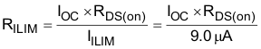
The OCP level is set by the ILIM pin voltage. A current (IILIM) is sourced into the ILIM pin from which a resistor RILIM is connected to GND. Resistor RILIM sets the first level of overcurrent limit. The OCP is based on the low-side FET voltage at the switch-node (SW pin) when LDRV is ON after a blanking time, which is the product of inductor current and low-side FET turnon resistance RDS(on). The voltage is inverted and compared to ILIM pin voltage. If it is greater than the ILIM pin voltage, then a 3-bit counter inside the device increments the fault-count by 1 at the start of the next switching cycle. Alternatively, if it is less than the ILIM pin voltage, then the counter inside the device decrements the fault-count by 1. When the fault-count reaches 7, an overcurrent fault (OC_FAULT) is declared and both the HDRV and LDRV are turned OFF. Resistor RILIM can be calculated by Equation 3.
The SCP level is set by a multiple of the ILIM pin voltage. The multiplier has three discrete values, 3, 7, or 15 times, which can be selected by choosing a 10-kΩ, open-circuit, or 20-kΩ resistor, respectively, from the LDRV pin to GND. This multiplier AOC information is translated during the tCAL time, which starts after the enable and UVLO conditions are met.
The SCP is based on sensing the high-side FET voltage drop from VVIN to VSW when HDRV is ON after a blanking time, which is product of inductor current and high-side FET turnon resistance RDS(on). The voltage is compared to the product of the multiplier and the ILIM pin voltage. If the voltage exceeds the product, then the fault-count is immediately set to 7 and the OC_FAULT is declared. HDRV is terminated immediately without waiting for the duty cycle to end. When an OC_FAULT is declared, both the HDRV and LDRV are turned OFF. The appropriate multiplier (A), can be selected using Equation 4.
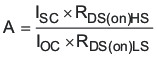
Figure 6-3 is a functional block diagram of the two-level overcurrent protection.
 Figure 6-3 OCP and SCP Protection Functional Block Diagram
Both OCP and SCP are based on low-side and high-side MOSFET voltage sensing at the SW node. Excessive ringing on the SW node can have a negative impact on the accuracy of OCP and SCP. Adding an R-C snubber from the SW node to GND helps minimize the potential impact.