SLVSB90C January 2012 – November 2023 TPS40170-Q1
PRODUCTION DATA
- 1
- 1 Features
- 2 Applications
- 3 Description
- 4 Pin Configuration and Functions
- 5 Specifications
-
6 Detailed Description
- 6.1 Overview
- 6.2 Functional Block Diagram
- 6.3
Feature Description
- 6.3.1 LDO Linear Regulators and Enable
- 6.3.2 Input Undervoltage Lockout (UVLO)
- 6.3.3 Equations for Programming the Input UVLO
- 6.3.4 Overcurrent Protection and Short-Circuit Protection (OCP and SCP)
- 6.3.5 Oscillator and Voltage Feed-Forward
- 6.3.6 Feed-Forward Oscillator Timing Diagram
- 6.3.7 Soft-Start and Fault-Logic
- 6.3.8 Overtemperature Fault
- 6.3.9 Tracking
- 6.3.10 Adaptive Drivers
- 6.3.11 Start-Up Into Pre-Biased Output
- 6.3.12 31
- 6.3.13 Power Good (PGOOD)
- 6.3.14 PGND and AGND
- 6.3.15 Bootstrap Capacitor
- 6.3.16 Bypass and Filtering
- 6.4 Device Functional Modes
-
7 Application and Implementation
- 7.1 Application Information
- 7.2
Typical Application
- 7.2.1 Design Requirements
- 7.2.2
Detailed Design Procedure
- 7.2.2.1 Select A Switching Frequency
- 7.2.2.2 Inductor Selection (L1)
- 7.2.2.3 Output Capacitor Selection (C9)
- 7.2.2.4 Peak Current Rating of Inductor
- 7.2.2.5 Input Capacitor Selection (C1, C6)
- 7.2.2.6 MOSFET Switch Selection (Q1, Q2)
- 7.2.2.7 Timing Resistor (R7)
- 7.2.2.8 UVLO Programming Resistors (R2, R6)
- 7.2.2.9 Bootstrap Capacitor (C7)
- 7.2.2.10 VIN Bypass Capacitor (C18)
- 7.2.2.11 VBP Bypass Capacitor (C19)
- 7.2.2.12 SS Timing Capacitor (C15)
- 7.2.2.13 ILIM Resistor (R19, C17)
- 7.2.2.14 SCP Multiplier Selection (R5)
- 7.2.2.15 Feedback Divider (R10, R11)
- 7.2.2.16 Compensation: (R4, R13, C13, C14, C21)
- 7.2.3 Application Curves
- 7.3 Power Supply Recommendations
- 7.4 Layout
- 8 Device and Documentation Support
- 9 Revision History
- 10Mechanical, Packaging, and Orderable Information
Package Options
Mechanical Data (Package|Pins)
- RGY|20
Thermal pad, mechanical data (Package|Pins)
- RGY|20
Orderable Information
7.2.2.5 Input Capacitor Selection (C1, C6)
The input voltage ripple is divided between capacitance and ESR. For this design, VRIPPLE(cap) = 400 mV and VRIPPLE(ESR) = 100 mV. The minimum capacitance and maximum ESR are estimated by:
Equation 27. 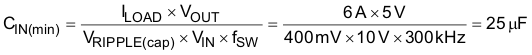
Equation 28. 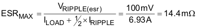
The rms current in the input capacitors is estimated in Equation 29.
Equation 29. 
To achieve these values, four 1210, 2.2-µF, 100-V, X7R ceramic capacitors plus a 120-µF electrolytic capacitor are combined at the input. This provides a smaller size and overall cost than 10 ceramic input capacitors or an electrolytic capacitor with the ESR required.
Table 7-3 Inductor Summary
| PARAMETER | VALUE | UNIT | |
|---|---|---|---|
| L | Inductance | 8.2 | µH |
| IL(rms) | RMS current (thermal rating) | 6.02 | A |
| IL(peak) | Peak current (saturation rating) | 7.01 | A |