SNVSBC0C September 2020 – December 2021 TPS542A50
PRODUCTION DATA
- 1 Features
- 2 Applications
- 3 Description
- 4 Revision History
- 5 Pin Configuration and Functions
- 6 Specifications
-
7 Detailed Description
- 7.1 Overview
- 7.2 Functional Block Diagram
- 7.3
Feature Description
- 7.3.1 Enable and Adjustable Undervoltage Lockout
- 7.3.2 Input and VREG Undervoltage Lockout Protection
- 7.3.3 Voltage Reference and Setting the Output Voltage
- 7.3.4 Remote Sense Function
- 7.3.5 Switching Frequency
- 7.3.6 Voltage Control Mode Internal Compensation
- 7.3.7 Soft Start and Prebiased Output Start-up
- 7.3.8 Power Good
- 7.3.9 Overvoltage and Undervoltage Protection
- 7.3.10 Overcurrent Protection
- 7.3.11 High-Side FET Throttling
- 7.3.12 Overtemperature Protection
- 7.4 Device Functional Modes
- 7.5 Programming
- 7.6 Pin-Strap Programming
- 7.7
Register Maps
- 7.7.1 ID Register (Offset = 0x0) [reset = 0x21]
- 7.7.2 STATUS Register (Offset = 0x1) [reset = 0x0]
- 7.7.3 VOUT_ADJ1 Register (Offset = 0x2) [reset = 0x0]
- 7.7.4 VOUT_ADJ2 Register (Offset = 0x3) [reset = 0x0]
- 7.7.5 CONFIG1 Register (Offset = 0x4) [reset = 0x0B]
- 7.7.6 CONFIG2 Register (Offset = 0x5) [reset = 0x2D]
-
8 Application and Implementation
- 8.1 Application Information
- 8.2
Typical Application
- 8.2.1
Full Analog Configuration
- 8.2.1.1 Design Requirements
- 8.2.1.2
Detailed Design Procedure
- 8.2.1.2.1 Custom Design With WEBENCH® Tools
- 8.2.1.2.2 Output Voltage Calculation
- 8.2.1.2.3 Switching Frequency Selection
- 8.2.1.2.4 Inductor Selection
- 8.2.1.2.5 Input Capacitor Selection
- 8.2.1.2.6 Bootstrap Capacitor Selection
- 8.2.1.2.7 R-C Snubber and VIN Pin High-Frequency Bypass
- 8.2.1.2.8 Output Capacitor Selection
- 8.2.1.2.9 Response to a Load Transient
- 8.2.1.2.10 Pin-Strap Setting
- 8.2.1.3 Application Curves
- 8.2.1.4 Typical Application Circuits
- 8.2.1
Full Analog Configuration
- 9 Power Supply Recommendations
- 10Layout
- 11Device and Documentation Support
- 12Mechanical, Packaging, and Orderable Information
Package Options
Mechanical Data (Package|Pins)
- RJM|33
Thermal pad, mechanical data (Package|Pins)
Orderable Information
8.2.1.2.5 Input Capacitor Selection
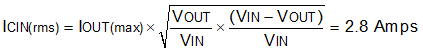
The TPS542A50 requires a high-quality, ceramic, type X5R or X7R, input decoupling capacitor with a value of at least 1 μF of effective capacitance on the PVIN pin, relative to PGND. The power stage input decoupling capacitance (effective capacitance at the PVIN and PGND pins) must be sufficient to supply the high switching currents demanded when the high-side MOSFET switches on, while providing minimal input voltage ripple as a result. This effective capacitance includes any DC bias effects. The voltage rating of the input capacitor must be greater than the maximum input voltage. The capacitor must also have a ripple current rating greater than the maximum input current ripple to the device during full load. The input ripple current can be calculated by Equation 4.
The minimum input capacitance and ESR values for a given input voltage ripple specification, VIN(ripple), are shown in Equation 5. The input ripple is composed of a capacitive portion, VIN(RIPPLE_CAP), and a resistive portion, VIN(RIPPLE_ESR).
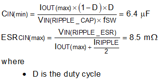
The value of a ceramic capacitor varies significantly over temperature and the amount of DC bias applied to the capacitor. The capacitance variations due to temperature can be minimized by selecting a dielectric material that is stable over temperature. X5R and X7R ceramic dielectrics are usually selected for power regulator capacitors because they have a high capacitance to volume ratio and are fairly stable over temperature. The input capacitor must also be selected with the DC bias taken into account. For this example design, a ceramic capacitor with at least a 25-V voltage rating is required to support the maximum input voltage. For this design, allow 0.1-V input ripple for VIN(RIPPLE_CAP), and 0.1-V input ripple for VIN(RIPPLE_ESR). UsingEquation 5, the minimum input capacitance for this design is 6.4 µF, and the maximum ESR is 8.5 mΩ. In a real application, it is recommended to use a combination of small capacitors such as 0.1 μF and larger value 10-μF or 22-μF ceramic capacitors in parallel for the power stage.