SNVSBC0C September 2020 – December 2021 TPS542A50
PRODUCTION DATA
- 1 Features
- 2 Applications
- 3 Description
- 4 Revision History
- 5 Pin Configuration and Functions
- 6 Specifications
-
7 Detailed Description
- 7.1 Overview
- 7.2 Functional Block Diagram
- 7.3
Feature Description
- 7.3.1 Enable and Adjustable Undervoltage Lockout
- 7.3.2 Input and VREG Undervoltage Lockout Protection
- 7.3.3 Voltage Reference and Setting the Output Voltage
- 7.3.4 Remote Sense Function
- 7.3.5 Switching Frequency
- 7.3.6 Voltage Control Mode Internal Compensation
- 7.3.7 Soft Start and Prebiased Output Start-up
- 7.3.8 Power Good
- 7.3.9 Overvoltage and Undervoltage Protection
- 7.3.10 Overcurrent Protection
- 7.3.11 High-Side FET Throttling
- 7.3.12 Overtemperature Protection
- 7.4 Device Functional Modes
- 7.5 Programming
- 7.6 Pin-Strap Programming
- 7.7
Register Maps
- 7.7.1 ID Register (Offset = 0x0) [reset = 0x21]
- 7.7.2 STATUS Register (Offset = 0x1) [reset = 0x0]
- 7.7.3 VOUT_ADJ1 Register (Offset = 0x2) [reset = 0x0]
- 7.7.4 VOUT_ADJ2 Register (Offset = 0x3) [reset = 0x0]
- 7.7.5 CONFIG1 Register (Offset = 0x4) [reset = 0x0B]
- 7.7.6 CONFIG2 Register (Offset = 0x5) [reset = 0x2D]
-
8 Application and Implementation
- 8.1 Application Information
- 8.2
Typical Application
- 8.2.1
Full Analog Configuration
- 8.2.1.1 Design Requirements
- 8.2.1.2
Detailed Design Procedure
- 8.2.1.2.1 Custom Design With WEBENCH® Tools
- 8.2.1.2.2 Output Voltage Calculation
- 8.2.1.2.3 Switching Frequency Selection
- 8.2.1.2.4 Inductor Selection
- 8.2.1.2.5 Input Capacitor Selection
- 8.2.1.2.6 Bootstrap Capacitor Selection
- 8.2.1.2.7 R-C Snubber and VIN Pin High-Frequency Bypass
- 8.2.1.2.8 Output Capacitor Selection
- 8.2.1.2.9 Response to a Load Transient
- 8.2.1.2.10 Pin-Strap Setting
- 8.2.1.3 Application Curves
- 8.2.1.4 Typical Application Circuits
- 8.2.1
Full Analog Configuration
- 9 Power Supply Recommendations
- 10Layout
- 11Device and Documentation Support
- 12Mechanical, Packaging, and Orderable Information
Package Options
Mechanical Data (Package|Pins)
- RJM|33
Thermal pad, mechanical data (Package|Pins)
Orderable Information
8.2.1.2.9 Response to a Load Transient
The output capacitance must supply the load with the required current when current is not immediately provided by the regulator. When the output capacitor supplies load current, the impedance of the capacitor greatly affects the magnitude of voltage deviation (such as undershoot and overshoot) during the transient.
Use Equation 6 and Equation 7 to calculate the minimum output capacitance to meet the undershoot and overshoot requirements. For this example, COUT(min_under) is 136 μF and 92 μF for COUT(min_over). In a real application, the value of a ceramic capacitor varies significantly over temperature and the amount of DC bias applied to the capacitor. It is recommended to check the capacitor datasheet and account for the capacitance derating.

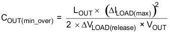
where
- COUT(min_under) is the minimum output capacitance to meet the undershoot requirement
- COUT(min_over)is the minimum output capacitance to meet the overshoot requirement
- D is the duty cycle
- L is the output inductance value (0.22 µH)
- ∆ILOAD(max) is the maximum transient step (5 A)
- VOUT is the output voltage value (1 V)
- tSW is the switching period (0.833 µs)
- VIN is the minimum input voltage for the design (12 V)
- ∆VLOAD(insert) is the undershoot requirement (30 mV)
- ∆VLOAD(release) is the overshoot requirement (30 mV)